- English
- Español
- Português
- русский
- Français
- 日本語
- Deutsch
- tiếng Việt
- Italiano
- Nederlands
- ภาษาไทย
- Polski
- 한국어
- Svenska
- magyar
- Malay
- বাংলা ভাষার
- Dansk
- Suomi
- हिन्दी
- Pilipino
- Türkçe
- Gaeilge
- العربية
- Indonesia
- Norsk
- تمل
- český
- ελληνικά
- український
- Javanese
- فارسی
- தமிழ்
- తెలుగు
- नेपाली
- Burmese
- български
- ລາວ
- Latine
- Қазақша
- Euskal
- Azərbaycan
- Slovenský jazyk
- Македонски
- Lietuvos
- Eesti Keel
- Română
- Slovenski
- मराठी
- Srpski језик
News
Heteroepitaxy of 3C-SiC: An Overview
The development of 3C-SiC, a significant polytype of silicon carbide, reflects the continuous advancement of semiconductor material science. In the 1980s, Nishino et al. first achieved a 4 μm thick 3C-SiC film on a silicon substrate using chemical vapor deposition (CVD)[1], laying the foundation for......
Read MoreHigh-Purity CVD Thick SiC: Process Insights for Material Growth
Thick, high-purity silicon carbide (SiC) layers, typically exceeding 1mm, are critical components in various high-value applications, including semiconductor fabrication and aerospace technologies. This article delves into the Chemical Vapor Deposition (CVD) process for producing such layers, highli......
Read MoreMonocrystalline silicon vs. polycrystalline silicon
Single crystal silicon and polycrystalline silicon each have their own unique advantages and applicable scenarios. Single crystal silicon is suitable for high-performance electronic products and microelectronics due to its excellent electrical and mechanical properties. Polycrystalline silicon, on t......
Read MoreSubstrate and Epitaxy
In the process of wafer preparation, there are two core links: one is the preparation of the substrate, and the other is the implementation of the epitaxial process. The substrate, a wafer carefully made of semiconductor single crystal material, can be directly put into the wafer manufacturing proce......
Read MoreUnderstanding Chemical Vapor Deposition (CVD): A Comprehensive Overview
Chemical Vapor Deposition (CVD) is a versatile thin-film deposition technique widely employed in the semiconductor industry for fabricating high-quality, conformal thin films on various substrates. This process involves chemical reactions of gaseous precursors onto a heated substrate surface, result......
Read MoreSilicon Wafer
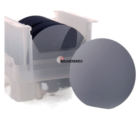
Silicon material is a solid material with certain semiconductor electrical properties and physical stability, and provides substrate support for the subsequent integrated circuit manufacturing process. It is a key material for silicon-based integrated circuits. More than 95% of semiconductor devices......
Read More
