
- English
- Español
- Português
- русский
- Français
- 日本語
- Deutsch
- tiếng Việt
- Italiano
- Nederlands
- ภาษาไทย
- Polski
- 한국어
- Svenska
- magyar
- Malay
- বাংলা ভাষার
- Dansk
- Suomi
- हिन्दी
- Pilipino
- Türkçe
- Gaeilge
- العربية
- Indonesia
- Norsk
- تمل
- český
- ελληνικά
- український
- Javanese
- فارسی
- தமிழ்
- తెలుగు
- नेपाली
- Burmese
- български
- ລາວ
- Latine
- Қазақша
- Euskal
- Azərbaycan
- Slovenský jazyk
- Македонски
- Lietuvos
- Eesti Keel
- Română
- Slovenski
- मराठी
- Srpski језик

Heteroepitaxy of 3C-SiC: An Overview
2024-07-29
1. Historical Development of 3C-SiC
The development of 3C-SiC, a significant polytype of silicon carbide, reflects the continuous advancement of semiconductor material science. In the 1980s, Nishino et al. first achieved a 4 μm thick 3C-SiC film on a silicon substrate using chemical vapor deposition (CVD)[1], laying the foundation for 3C-SiC thin-film technology.
The 1990s marked a golden age for SiC research. Cree Research Inc.’s launch of 6H-SiC and 4H-SiC chips in 1991 and 1994, respectively, propelled the commercialization of SiC semiconductor devices. This technological progress laid the groundwork for subsequent research and applications of 3C-SiC.
In the early 21st century, silicon-based SiC films also saw significant progress in China. Ye Zhizhen et al. fabricated SiC films on silicon substrates using CVD at low temperatures in 2002[2], while An Xia et al. achieved similar results using magnetron sputtering at room temperature in 2001[3].
However, the large lattice mismatch between Si and SiC (approximately 20%) led to a high defect density in the 3C-SiC epitaxial layer, particularly double positioning boundaries (DPBs). To mitigate this, researchers opted for substrates like 6H-SiC, 15R-SiC, or 4H-SiC with a (0001) orientation for growing 3C-SiC epitaxial layers, thereby reducing defect density. For instance, in 2012, Seki, Kazuaki et al. proposed a kinetic polymorphism control technique, achieving selective growth of 3C-SiC and 6H-SiC on 6H-SiC(0001) seeds by controlling supersaturation[4-5]. In 2023, Xun Li et al. successfully obtained smooth 3C-SiC epitaxial layers free of DPBs on 4H-SiC substrates using optimized CVD growth with a rate of 14 μm/h[6].
2. Crystal Structure and Applications of 3C-SiC
Among the numerous SiC polytypes, 3C-SiC, also known as β-SiC, is the only cubic polytype. In this crystal structure, Si and C atoms exist in a one-to-one ratio, forming a tetrahedral unit cell with strong covalent bonds. The structure is characterized by Si-C bilayers arranged in an ABC-ABC-… sequence, with each unit cell containing three such bilayers, denoted by the C3 notation. Figure 1 illustrates the crystal structure of 3C-SiC.
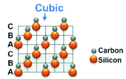
Figure 1. Crystal structure of 3C-SiC
Currently, silicon (Si) is the most widely used semiconductor material for power devices. However, its inherent limitations restrict its performance. Compared to 4H-SiC and 6H-SiC, 3C-SiC possesses the highest theoretical electron mobility at room temperature (1000 cm2·V-1·s-1), making it more advantageous for MOSFET applications. Additionally, its high breakdown voltage, excellent thermal conductivity, high hardness, wide bandgap, high-temperature resistance, and radiation resistance make 3C-SiC highly promising for applications in electronics, optoelectronics, sensors, and extreme environments:
High-Power, High-Frequency, and High-Temperature Applications: 3C-SiC’s high breakdown voltage and high electron mobility make it ideal for manufacturing power devices like MOSFETs, particularly in demanding environments[7].
Nanoelectronics and Microelectromechanical Systems (MEMS): Its compatibility with silicon technology allows for the fabrication of nanoscale structures, enabling applications in nanoelectronics and MEMS devices[8].
Optoelectronics: As a wide-bandgap semiconductor material, 3C-SiC is suitable for blue light-emitting diodes (LEDs). Its high luminous efficiency and ease of doping make it attractive for applications in lighting, display technologies, and lasers[9].
Sensors: 3C-SiC is employed in position-sensitive detectors, particularly laser spot position-sensitive detectors based on the lateral photovoltaic effect. These detectors exhibit high sensitivity under zero bias conditions, making them suitable for precision positioning applications[10].
3. Preparation Methods for 3C-SiC Heteroepitaxy
Common methods for 3C-SiC heteroepitaxy include chemical vapor deposition (CVD), sublimation epitaxy (SE), liquid phase epitaxy (LPE), molecular beam epitaxy (MBE), and magnetron sputtering. CVD is the preferred method for 3C-SiC epitaxy due to its controllability and adaptability in terms of temperature, gas flow, chamber pressure, and reaction time, enabling optimization of the epitaxial layer quality.
Chemical Vapor Deposition (CVD): Gaseous compounds containing Si and C are introduced into a reaction chamber and heated to high temperatures, leading to their decomposition. The Si and C atoms then deposit onto a substrate, typically Si, 6H-SiC, 15R-SiC, or 4H-SiC [11]. This reaction typically occurs between 1300-1500°C. Common Si sources include SiH4, TCS, and MTS, while C sources are primarily C2H4 and C3H8, with H2 as the carrier gas. Figure 2 depicts a schematic of the CVD process[12].
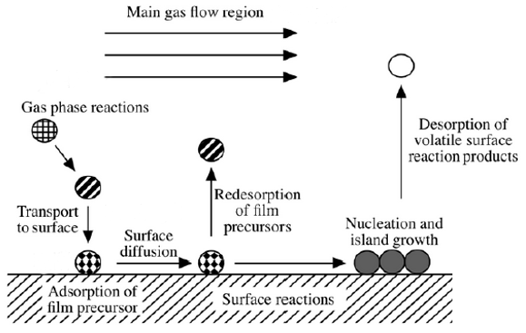
Figure 2. Schematic of the CVD process
Sublimation Epitaxy (SE): In this method, a 6H-SiC or 4H-SiC substrate is placed at the top of a crucible, with high-purity SiC powder as the source material at the bottom. The crucible is heated to 1900-2100°C via radio frequency induction, maintaining the substrate temperature lower than the source temperature to create an axial temperature gradient. This allows sublimated SiC to condense and crystallize on the substrate, forming the 3C-SiC heteroepitaxy.
Molecular Beam Epitaxy (MBE): This advanced thin-film growth technique is suitable for growing 3C-SiC epitaxial layers on 4H-SiC or 6H-SiC substrates. Under ultra-high vacuum, precise control of source gases enables the formation of directional atomic or molecular beams of constituent elements. These beams are directed towards the heated substrate surface for epitaxial growth.
4. Conclusion and Outlook
With continuous technological advancements and in-depth mechanistic studies, 3C-SiC heteroepitaxy is poised to play an increasingly vital role in the semiconductor industry, driving the development of energy-efficient electronic devices. Exploring new growth techniques, such as introducing HCl atmospheres to enhance growth rates while maintaining low defect densities, is a promising avenue for future research. Further investigation into defect formation mechanisms and the development of advanced characterization techniques will enable precise defect control and optimized material properties. Rapid growth of high-quality, thick 3C-SiC films is crucial for meeting the demands of high-voltage devices, requiring further research to address the balance between growth rate and material uniformity. By leveraging the applications of 3C-SiC in heterostructures like SiC/GaN, its potential in novel devices such as power electronics, optoelectronic integration, and quantum information processing can be fully explored.
References:
[1] Nishino S , Hazuki Y , Matsunami H ,et al. Chemical Vapor Deposition of Single Crystalline β‐SiC Films on Silicon Substrate with Sputtered SiC Intermediate Layer[J].Journal of The Electrochemical Society, 1980, 127(12):2674-2680.
[2]叶志镇,王亚东,黄靖云,等.低温生长硅基碳化硅薄膜研究[J].真空科学与技术学报, 2002, 022(001):58-60.
[3]安霞,庄惠照,李怀祥,等.在(111)Si衬底上磁控溅射法制备纳米SiC薄膜[J].山东师范大学学报:自然科学版, 2001: 382-384..
[4] Seki K, Alexander, Kozawa S, et al. Polytype-selective growth of SiC by supersaturation control in solution growth[J]. Journal of Crystal Growth, 2012, 360:176-180.
[5] 陈尧,赵富强,朱炳先,贺帅.国内外碳化硅功率器件发展综述[J].车辆与动力技术,2020:49-54.
[6] Li X , Wang G .CVD growth of 3C-SiC layers on 4H-SiC substrates with improved morphology[J].Solid State Communications, 2023:371.
[7] 侯凯文. Si 图形化衬底研究及其在 3C-SiC 生长上的应用[D]. 西安理工大学, 2018.
[8]Lars, Hiller , Thomas, et al. Hydrogen Effects in ECR-Etching of 3C-SiC(100) Mesa Structures[J].Materials Science Forum, 2014.
[9]徐青芳.激光化学气相沉积法制备-3C-SiC薄膜[D].武汉理工大学,2016.
[10] Foisal A R M , Nguyen T , Dinh T K ,et al.3C-SiC/Si Heterostructure: An Excellent Platform for Position-Sensitive Detectors Based on Photovoltaic Effect[J].ACS Applied Materials & Interfaces, 2019: 40980-40987.
[11] 辛斌. 基于CVD工艺的3C/4H-SiC异质外延:缺陷表征及演化[D].西安电子科技大学.
[12] 董林. 碳化硅大面积多片外延生长技术及物性表征[D].中国科学院大学, 2014.
[13] Diani M , Simon L , Kubler L ,et al. Crystal growth of 3C-SiC polytype on 6H-SiC(0001) substrate[J]. Journal of Crystal Growth, 2002, 235(1):95-102.


