- English
- Español
- Português
- русский
- Français
- 日本語
- Deutsch
- tiếng Việt
- Italiano
- Nederlands
- ภาษาไทย
- Polski
- 한국어
- Svenska
- magyar
- Malay
- বাংলা ভাষার
- Dansk
- Suomi
- हिन्दी
- Pilipino
- Türkçe
- Gaeilge
- العربية
- Indonesia
- Norsk
- تمل
- český
- ελληνικά
- український
- Javanese
- فارسی
- தமிழ்
- తెలుగు
- नेपाली
- Burmese
- български
- ລາວ
- Latine
- Қазақша
- Euskal
- Azərbaycan
- Slovenský jazyk
- Македонски
- Lietuvos
- Eesti Keel
- Română
- Slovenski
- मराठी
- Srpski језик

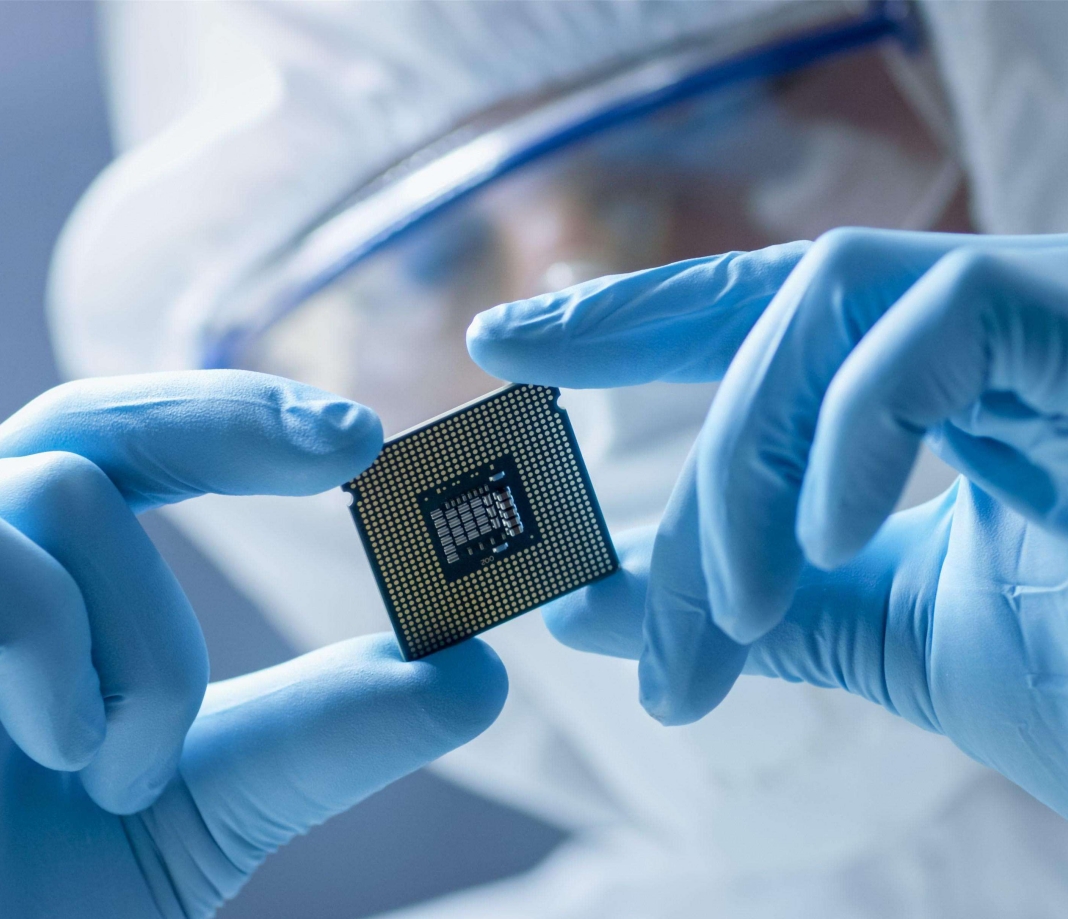
Thin film growth process
2024-07-29
Common thin films are mainly divided into three categories: semiconductor thin films, dielectric thin films, and metal/metal compound thin films.
Semiconductor thin films: mainly used to prepare the channel region of the source/drain, single crystal epitaxial layer and MOS gate, etc.
Dielectric thin films: mainly used for shallow trench isolation, gate oxide layer, side wall, barrier layer, metal layer front dielectric layer, back-end metal layer dielectric layer, etch stop layer, barrier layer, anti-reflection layer, passivation layer, etc., and can also be used for hard mask.
Metal and metal compound thin films: metal thin films are mainly used for metal gates, metal layers, and pads, and metal compound thin films are mainly used for barrier layers, hard masks, etc.
Thin film deposition methods
The deposition of thin films requires different technical principles, and different deposition methods such as physics and chemistry need to complement each other. Thin film deposition processes are mainly divided into two categories: physical and chemical.
Physical methods include thermal evaporation and sputtering. Thermal evaporation refers to the material transfer of atoms from the source material to the surface of the wafer substrate material by heating the evaporation source to evaporate it. This method is fast, but the film has poor adhesion and poor step properties. Sputtering is to pressurize and ionize the gas (argon gas) to become a plasma, bombard the target material to make its atoms fall off and fly to the substrate surface to achieve transfer. Sputtering has strong adhesion, good step properties and good density.
The chemical method is to introduce the gaseous reactant containing the elements that constitute the thin film into the process chamber with different partial pressures of gas flow, chemical reaction occurs on the substrate surface and a thin film is deposited on the substrate surface.
Physical methods are mainly used to deposit metal wires and metal compound films, while general physical methods cannot achieve the transfer of insulating materials. Chemical methods are required to deposit through reactions between different gases. In addition, some chemical methods can also be used to deposit metal films.
ALD/Atomic Layer Deposition refers to the deposition of atoms layer by layer on the substrate material by growing a single atomic film layer by layer, which is also a chemical method. It has good step coverage, uniformity, and consistency, and can better control the film thickness, composition, and structure.
Semicorex offers high-quality SiC/TaC coated graphite parts for epitaxial layer growth. If you have any inquiries or need additional details, please don't hesitate to get in touch with us.
Contact phone # +86-13567891907
Email: sales@semicorex.com
Previous:Heteroepitaxy of 3C-SiC: An Overview