
- English
- Español
- Português
- русский
- Français
- 日本語
- Deutsch
- tiếng Việt
- Italiano
- Nederlands
- ภาษาไทย
- Polski
- 한국어
- Svenska
- magyar
- Malay
- বাংলা ভাষার
- Dansk
- Suomi
- हिन्दी
- Pilipino
- Türkçe
- Gaeilge
- العربية
- Indonesia
- Norsk
- تمل
- český
- ελληνικά
- український
- Javanese
- فارسی
- தமிழ்
- తెలుగు
- नेपाली
- Burmese
- български
- ລາວ
- Latine
- Қазақша
- Euskal
- Azərbaycan
- Slovenský jazyk
- Македонски
- Lietuvos
- Eesti Keel
- Română
- Slovenski
- मराठी
- Srpski језик

Substrate and Epitaxy
2024-07-26
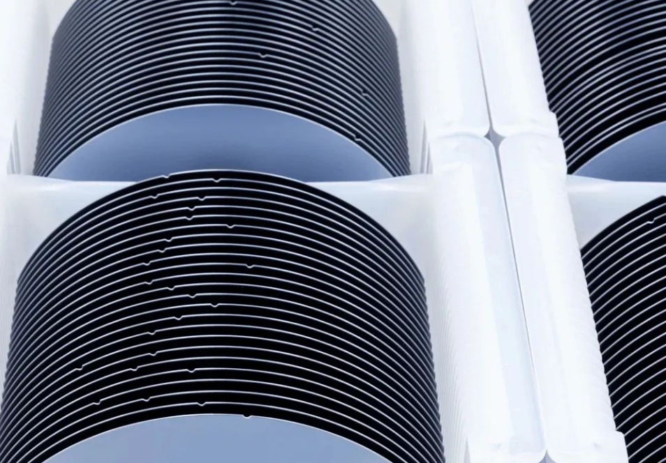
In the process of wafer preparation, there are two core links: one is the preparation of the substrate, and the other is the implementation of the epitaxial process. The substrate, a wafer carefully made of semiconductor single crystal material, can be directly put into the wafer manufacturing process as a basis to produce semiconductor devices, or further enhance the performance through the epitaxial process.
So, what is epitaxy? In short, epitaxy is to grow a new layer of single crystal on a single crystal substrate that has been finely processed (cutting, grinding, polishing, etc.). This new single crystal and the substrate can be made of the same material or different materials, so that homogeneous or heterogeneous epitaxy can be achieved as needed. Because the newly grown single crystal layer will expand according to the crystal phase of the substrate, it is called an epitaxial layer. Its thickness is generally only a few microns. Taking silicon as an example, silicon epitaxial growth is to grow a layer of silicon single crystal layer with the same crystal orientation as the substrate, controllable resistivity and thickness, and perfect lattice structure on a silicon single crystal substrate with a specific crystal orientation. When the epitaxial layer grows on the substrate, the whole is called an epitaxial wafer.
For the traditional silicon semiconductor industry, making high-frequency and high-power devices directly on silicon wafers will encounter some technical difficulties, such as the high breakdown voltage, small series resistance and small saturation voltage drop in the collector region are difficult to achieve. The introduction of epitaxial technology cleverly solves these problems. The solution is to grow a high-resistivity epitaxial layer on a low-resistivity silicon substrate, and then make devices on the high-resistivity epitaxial layer. In this way, the high-resistivity epitaxial layer provides a high breakdown voltage for the device, while the low-resistivity substrate reduces the resistance of the substrate, thereby reducing the saturation voltage drop, thereby achieving a balance between high breakdown voltage and low resistance and low voltage drop.
In addition, epitaxial technologies such as vapor phase epitaxy and liquid phase epitaxy of III-V, II-VI and other molecular compound semiconductor materials such as GaAs have also been greatly developed and have become indispensable process technologies for the production of most microwave devices, optoelectronic devices, power devices, etc., especially the successful application of molecular beam and metal organic vapor phase epitaxy in thin layers, superlattices, quantum wells, strained superlattices, and atomic thin layer epitaxy, which has laid a solid foundation for the development of "band engineering", a new field of semiconductor research.
As for the third-generation semiconductor devices, such semiconductor devices are almost all made on the epitaxial layer, and the silicon carbide wafer itself is only used as a substrate. Parameters such as the thickness and background carrier concentration of SiC epitaxial materials directly determine the various electrical properties of SiC devices. Silicon carbide devices for high voltage applications put forward new requirements for parameters such as the thickness and background carrier concentration of epitaxial materials. Therefore, silicon carbide epitaxial technology plays a decisive role in fully exerting the performance of silicon carbide devices. Almost all SiC power devices are prepared based on high-quality SiC epitaxial wafers, and the production of epitaxial layers is an important part of the wide bandgap semiconductor industry.
Previous:Silicon Wafer


