
- English
- Español
- Português
- русский
- Français
- 日本語
- Deutsch
- tiếng Việt
- Italiano
- Nederlands
- ภาษาไทย
- Polski
- 한국어
- Svenska
- magyar
- Malay
- বাংলা ভাষার
- Dansk
- Suomi
- हिन्दी
- Pilipino
- Türkçe
- Gaeilge
- العربية
- Indonesia
- Norsk
- تمل
- český
- ελληνικά
- український
- Javanese
- فارسی
- தமிழ்
- తెలుగు
- नेपाली
- Burmese
- български
- ລາວ
- Latine
- Қазақша
- Euskal
- Azərbaycan
- Slovenský jazyk
- Македонски
- Lietuvos
- Eesti Keel
- Română
- Slovenski
- मराठी
- Srpski језик

Silicon Wafer
2024-07-19
Silicon material is a solid material with certain semiconductor electrical properties and physical stability, and provides substrate support for the subsequent integrated circuit manufacturing process. It is a key material for silicon-based integrated circuits. More than 95% of semiconductor devices and more than 90% of integrated circuits in the world are made on silicon wafers.
According to the different single crystal growth methods, silicon single crystals are divided into two types: Czochralski (CZ) and floating zone (FZ). Silicon wafers can be roughly divided into three categories: polished wafers, epitaxial wafers, and Silicon-On-insulator(SOI).
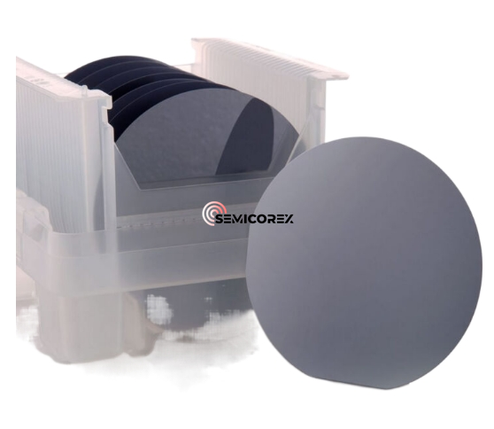
Silicon polishing wafer refers to a silicon wafer formed by polishing the surface. It is a round wafer with a thickness of less than 1mm processed by cutting, grinding, polishing, cleaning and other processes of a single crystal rod. It is mainly used in integrated circuits and discrete devices and occupies an important position in the semiconductor industry chain.
When V group elements such as phosphorus, antimony, arsenic, etc. are doped into silicon single crystals, N-type conductive materials will be formed; when III group elements such as boron are doped into silicon, P-type conductive materials will be formed. The resistivity of silicon single crystals is determined by the amount of doping elements doped. The greater the doping amount, the lower the resistivity. Lightly doped silicon polishing wafers generally refer to silicon polishing wafers with a resistivity of more than 0.1W·cm, which are widely used in the manufacture of large-scale integrated circuits and memory; heavily doped silicon polishing wafers generally refer to silicon polishing wafers with a resistivity of less than 0.1W·cm, which are generally used as substrate materials for epitaxial silicon wafers and are widely used in the manufacture of semiconductor power devices.
Silicon polishing wafers that form a clean area on the surface of silicon wafers after annealing heat treatment are called silicon annealing wafers. Commonly used ones are hydrogen annealing wafers and argon annealing wafers. 300mm silicon wafers and some 200mm silicon wafers with higher requirements require the use of double-sided polishing process. Therefore, the external gettering technology that introduces the gettering center through the back of the silicon wafer is difficult to apply. The internal gettering process that uses the annealing process to form the internal gettering center has become the mainstream gettering process for large-size silicon wafers. Compared with general polished wafers, annealed wafers can improve device performance and increase yield, and are widely used in the manufacture of digital and analog integrated circuits and memory chips.
The basic principle of zone melting single crystal growth is to rely on the surface tension of the melt to suspend the molten zone between the polycrystalline silicon rod and the single crystal grown below, and purify and grow silicon single crystals by moving the molten zone upward. Zone melting silicon single crystals are not contaminated by crucibles and have high purity. They are suitable for the production of N-type silicon single crystals (including neutron transmutation doped single crystals) with resistivity higher than 200Ω·cm and high-resistance P-type silicon single crystals. Zone melting silicon single crystals are mainly used in the manufacture of high-voltage and high-power devices.
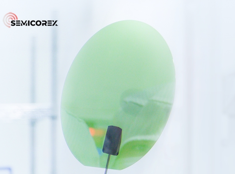
Silicon epitaxial wafer refers to a material on which one or more layers of silicon single crystal thin film are grown by vapor phase epitaxial deposition on a substrate, and is mainly used to manufacture various integrated circuits and discrete devices.
In advanced CMOS integrated circuit processes, in order to improve the integrity of the gate oxide layer, improve leakage in the channel, and enhance the reliability of integrated circuits, silicon epitaxial wafers are often used, that is, a layer of silicon thin film is homogeneously epitaxial grown on a lightly doped silicon polished wafer, which can avoid the shortcomings of high oxygen content and many defects on the surface of general silicon polished wafers; while for silicon epitaxial wafers used for power integrated circuits and discrete devices, a layer of high resistivity epitaxial layer is usually epitaxial grown on a low resistivity silicon substrate (heavily doped silicon polished wafer). In high-power and high-voltage application environments, the low resistivity of the silicon substrate can reduce the on-resistance, and the high-resistivity epitaxial layer can increase the breakdown voltage of the device.
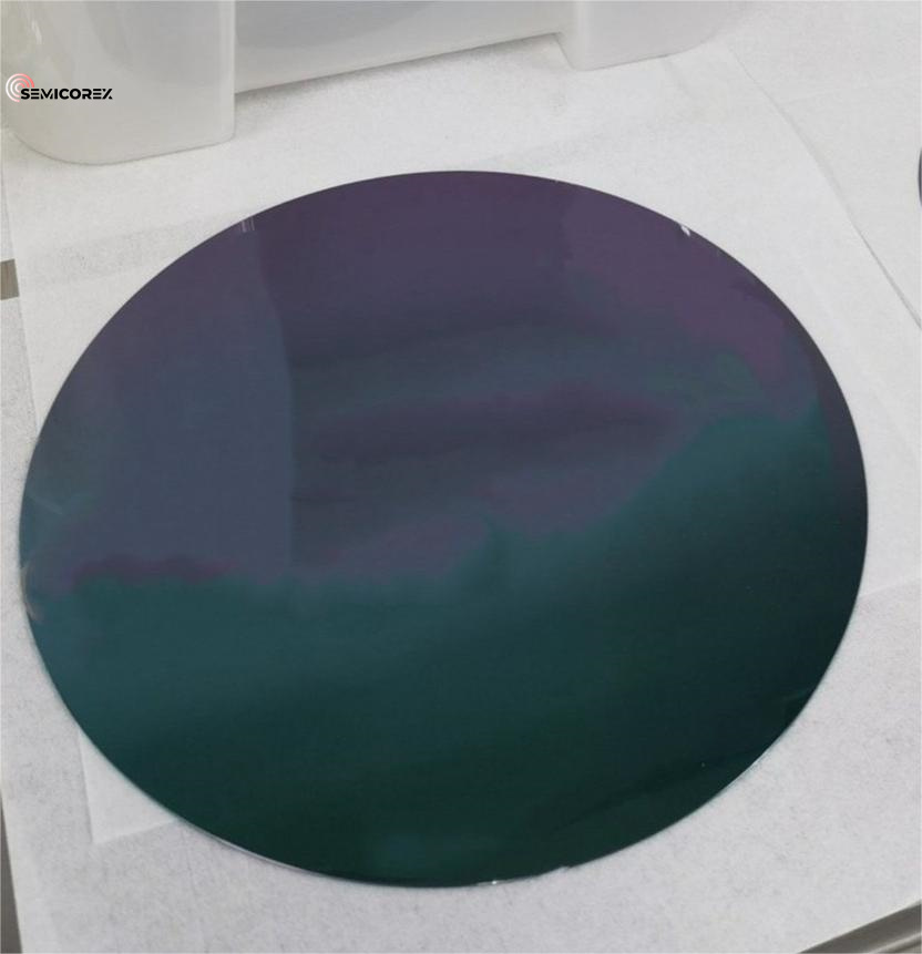
SOI (Silicon-On-Insulator) is silicon on an insulating layer. It is a "sandwich" structure with a top silicon layer (Top Silicon), a middle silicon dioxide buried layer (BOX) and a silicon substrate support (Handle) below. As a new substrate material for integrated circuit manufacturing, the main advantage of SOI is that it can achieve high electrical insulation through the oxide layer, which will effectively reduce the parasitic capacitance and leakage of silicon wafers, which is conducive to the production of high-speed, low-power, high-integration and high-reliability ultra-large-scale integrated circuits, and is widely used in high-voltage power devices, optical passive devices, MEMS and other fields. At present, the preparation technology of SOI materials mainly includes bonding technology (BESOI), smart stripping technology (Smart-Cut), oxygen ion implantation technology (SIMOX), oxygen injection bonding technology (Simbond), etc. The most mainstream technology is smart stripping technology.
SOI silicon wafers can be further divided into thin-film SOI silicon wafers and thick-film SOI silicon wafers. The thickness of the top silicon of thin-film SOI silicon wafers is less than 1um. At present, 95% of the thin-film SOI silicon wafer market is concentrated in 200mm and 300mm sizes, and its market driving force mainly comes from high-speed, low-power products, especially in microprocessor applications. For example, in advanced processes below 28nm, fully depleted silicon on insulator (FD-SOI) has obvious performance advantages of low power consumption, radiation protection, and high temperature resistance. At the same time, the use of SOI solutions can greatly reduce the manufacturing process. The top silicon thickness of thick-film SOI silicon wafers is greater than 1um, and the buried layer thickness is 0.5-4um. It is mainly used in power devices and MEMS fields, especially in industrial control, automotive electronics, wireless communications, etc., and usually uses 150mm and 200mm diameter products.
Previous:SiC Cutting


