
- English
- Español
- Português
- русский
- Français
- 日本語
- Deutsch
- tiếng Việt
- Italiano
- Nederlands
- ภาษาไทย
- Polski
- 한국어
- Svenska
- magyar
- Malay
- বাংলা ভাষার
- Dansk
- Suomi
- हिन्दी
- Pilipino
- Türkçe
- Gaeilge
- العربية
- Indonesia
- Norsk
- تمل
- český
- ελληνικά
- український
- Javanese
- فارسی
- தமிழ்
- తెలుగు
- नेपाली
- Burmese
- български
- ລາວ
- Latine
- Қазақша
- Euskal
- Azərbaycan
- Slovenský jazyk
- Македонски
- Lietuvos
- Eesti Keel
- Română
- Slovenski
- मराठी
- Srpski језик

Understanding Chemical Vapor Deposition (CVD): A Comprehensive Overview
2024-07-22
1. Mechanism of CVD
CVD involves a series of complex, interlinked steps that govern the formation of thin films. These steps are highly dependent on the specific reactants involved and the chosen process conditions. However, a general framework for understanding CVD reactions can be outlined as follows:
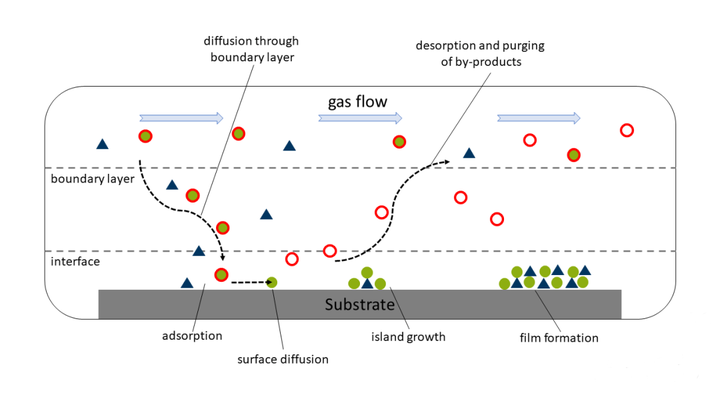
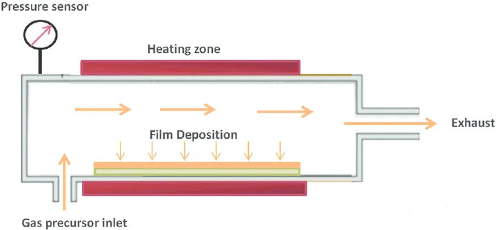
Precursor Introduction and Activation: Gaseous precursor materials are introduced into the reaction chamber. These precursors are then activated, typically through heating, plasma generation, or a combination of both.
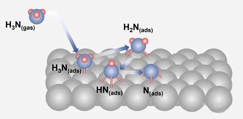
Surface Reaction: Activated precursor molecules adsorb onto the heated substrate surface. Subsequently, they undergo chemical reactions, leading to the formation of the desired thin film material. These reactions can encompass a variety of chemical processes, including oxidation, reduction, decomposition, and chemical vapor deposition.
Film Growth: As the process continues, a continuous supply of activated precursor molecules sustains the reaction at the substrate surface, leading to the gradual buildup and growth of the thin film. The film growth rate is influenced by factors such as reaction temperature, pressure, and precursor concentration.
Adhesion and Crystallization: The deposited material adheres to the substrate surface and undergoes crystallization, forming a continuous, solid thin film with specific morphology and crystal structure. The properties of the deposited film are dictated by the chosen deposition parameters and the intrinsic characteristics of the precursor materials.
2. Process Conditions and Precursors
CVD processes typically require elevated temperatures and pressures to facilitate the chemical reactions involved in thin film deposition. High temperatures enhance the reactivity of precursor molecules, promoting efficient film formation. Elevated pressures increase the concentration of reactants near the substrate surface, further accelerating the deposition rate.

A diverse range of chemical precursors can be employed in CVD processes, encompassing gases, liquids, and solids. Commonly used precursors include:
Oxygen: Often used as an oxidizing agent in oxide film deposition.
Halides: Examples include silicon tetrachloride (SiCl4), tungsten hexafluoride (WF6), and titanium tetrachloride (TiCl4).
Hydrides: Silane (SiH4), germane (GeH4), and ammonia (NH3) are common examples.
Organometallics: These include trimethylaluminum (Al(CH3)3) and tetrakis(dimethylamido)titanium (Ti(NMe2)4).
Metal Alkoxides: Tetraethyl orthosilicate (TEOS) and titanium isopropoxide (Ti(OiPr)4) are examples.
The purity of precursor materials is paramount in CVD processes. Impurities present in precursors can incorporate into the deposited film, altering its properties and potentially degrading device performance. Furthermore, CVD precursors should exhibit stability under storage conditions to prevent decomposition and subsequent impurity formation.
3. Advantages of CVD
CVD offers several advantages over other thin-film deposition techniques, contributing to its widespread adoption in semiconductor manufacturing:
High Conformality: CVD excels in depositing uniform films even on complex, three-dimensional structures with high aspect ratios. This attribute makes it invaluable for coating trenches, vias, and other intricate features commonly encountered in semiconductor devices.
Cost-Effectiveness: CVD often proves more cost-effective compared to Physical Vapor Deposition (PVD) techniques, such as sputtering, due to its higher deposition rates and the ability to achieve thick coatings.
Versatile Process Control: CVD offers a wide processing window, allowing for precise control over film thickness, composition, and uniformity by adjusting process parameters like temperature, pressure, and precursor flow rates.
4. Limitations of CVD
Despite its advantages, CVD does present certain limitations:
High Processing Temperatures: The requirement for elevated temperatures can be a limiting factor for substrates with low thermal stability.
Precursor Toxicity and Safety: Many CVD precursors are toxic, flammable, or corrosive, necessitating stringent safety protocols during handling and disposal.
Waste Management: The byproducts of CVD reactions can be hazardous and require careful treatment and disposal.
5. Comparison with PVD Coatings
PVD and CVD represent two distinct approaches to thin film deposition, each with its own set of advantages and limitations. PVD techniques, such as sputtering and evaporation, involve the physical transfer of material from a target to the substrate in a vacuum environment. In contrast, CVD relies on chemical reactions of gaseous precursors at the substrate surface.
Key differences include:
Material Compatibility: PVD can deposit a wider range of materials, including metals, alloys, and ceramics, while CVD is typically more suitable for depositing ceramics and some polymers.
Process Conditions: PVD processes typically occur under high vacuum, while CVD can operate at a wider range of pressures.
Coating Properties: PVD coatings tend to be thinner and less conformal compared to CVD coatings. However, PVD offers advantages in terms of deposition speed and versatility in coating complex geometries.
6. Conclusion
Chemical Vapor Deposition (CVD) stands as a cornerstone technology in semiconductor manufacturing, enabling the deposition of high-quality thin films with exceptional uniformity, conformality, and control over material properties. Its ability to deposit a wide range of materials, combined with its cost-effectiveness and scalability, makes it an indispensable tool for fabricating advanced semiconductor devices. As the demand for miniaturization and performance continues to drive the semiconductor industry forward, CVD will undoubtedly remain a critical enabling technology for years to come.**


