
- English
- Español
- Português
- русский
- Français
- 日本語
- Deutsch
- tiếng Việt
- Italiano
- Nederlands
- ภาษาไทย
- Polski
- 한국어
- Svenska
- magyar
- Malay
- বাংলা ভাষার
- Dansk
- Suomi
- हिन्दी
- Pilipino
- Türkçe
- Gaeilge
- العربية
- Indonesia
- Norsk
- تمل
- český
- ελληνικά
- український
- Javanese
- فارسی
- தமிழ்
- తెలుగు
- नेपाली
- Burmese
- български
- ລາວ
- Latine
- Қазақша
- Euskal
- Azərbaycan
- Slovenský jazyk
- Македонски
- Lietuvos
- Eesti Keel
- Română
- Slovenski
- मराठी
- Srpski језик

High-Purity CVD Thick SiC: Process Insights for Material Growth
2024-07-26
1. Conventional CVD SiC Deposition Process
The standard CVD process for depositing SiC coatings involves a series of carefully controlled steps:
Heating: The CVD furnace is heated to a temperature between 100-160°C.
Substrate Loading: A graphite substrate (mandrel) is placed on a rotating platform within the deposition chamber.
Vacuum and Purging: The chamber is evacuated and purged with argon (Ar) gas in multiple cycles.
Heating and Pressure Control: The chamber is heated to the deposition temperature under continuous vacuum. After reaching the desired temperature, a holding time is maintained before introducing Ar gas to achieve a pressure of 40-60 kPa. The chamber is then evacuated again.
Precursor Gas Introduction: A mixture of hydrogen (H2), argon (Ar), and a hydrocarbon gas (alkane) is introduced into a preheating chamber, along with a chlorosilane precursor (typically silicon tetrachloride, SiCl4). The resulting gas mixture is then fed into the reaction chamber.
Deposition and Cooling: Upon completion of the deposition, the H2, chlorosilane, and alkane flow are stopped. Argon flow is maintained to purge the chamber while cooling. Finally, the chamber is brought to atmospheric pressure, opened, and the SiC-coated graphite substrate is removed.
2. Applications of Thick CVD SiC Layers
High-density SiC layers exceeding 1mm thickness find critical applications in:
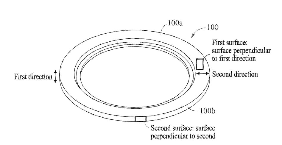
Semiconductor Manufacturing: As focus rings (FR) in dry etch systems for integrated circuit fabrication.
Optics and Aerospace: High-transparency SiC layers are utilized in optical mirrors and spacecraft windows.
These applications demand high-performance materials, making thick SiC a high-value product with significant economic potential.
3. Target Characteristics for Semiconductor-Grade CVD SiC
CVD SiC for semiconductor applications, particularly for focus rings, requires stringent material properties:
High Purity: Polycrystalline SiC with a purity level of 99.9999% (6N).
High Density: A dense, pore-free microstructure is essential.
High Thermal Conductivity: Theoretical values approach 490 W/m·K, with practical values ranging from 200-400 W/m·K.
Controlled Electrical Resistivity: Values between 0.01-500 Ω.cm are desirable.
Plasma Resistance and Chemical Inertness: Critical for withstanding aggressive etching environments.
High Hardness: SiC’s inherent hardness (~3000 kg/mm2) necessitates specialized machining techniques.
Cubic Polycrystalline Structure: Preferentially oriented 3C-SiC (β-SiC) with a dominant (111) crystallographic orientation is desired.
4. CVD Process for 3C-SiC Thick Films
The preferred method for depositing thick 3C-SiC films for focus rings is CVD, using the following parameters:
Precursor Selection: Methyltrichlorosilane (MTS) is commonly used, offering a 1:1 Si/C molar ratio for stoichiometric deposition. However, some manufacturers optimize the Si:C ratio (1:1.1 to 1:1.4) to enhance plasma resistance, potentially impacting grain size distribution and preferred orientation.
Carrier Gas: Hydrogen (H2) reacts with chlorine-containing species, while argon (Ar) acts as a carrier gas for MTS and dilutes the gas mixture to control the deposition rate.
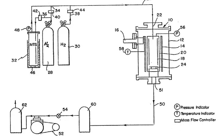
5. CVD System for Focus Ring Applications
A schematic representation of a typical CVD system for depositing 3C-SiC for focus rings is presented. However, detailed production systems are often custom-designed and proprietary.
6. Conclusion
The production of high-purity, thick SiC layers via CVD is a complex process requiring precise control over numerous parameters. As the demand for these high-performance materials continues to rise, ongoing research and development efforts focus on optimizing CVD techniques to meet the stringent requirements of next-generation semiconductor fabrication and other demanding applications.**


