- English
- Español
- Português
- русский
- Français
- 日本語
- Deutsch
- tiếng Việt
- Italiano
- Nederlands
- ภาษาไทย
- Polski
- 한국어
- Svenska
- magyar
- Malay
- বাংলা ভাষার
- Dansk
- Suomi
- हिन्दी
- Pilipino
- Türkçe
- Gaeilge
- العربية
- Indonesia
- Norsk
- تمل
- český
- ελληνικά
- український
- Javanese
- فارسی
- தமிழ்
- తెలుగు
- नेपाली
- Burmese
- български
- ລາວ
- Latine
- Қазақша
- Euskal
- Azərbaycan
- Slovenský jazyk
- Македонски
- Lietuvos
- Eesti Keel
- Română
- Slovenski
- मराठी
- Srpski језик
ESC Chuck
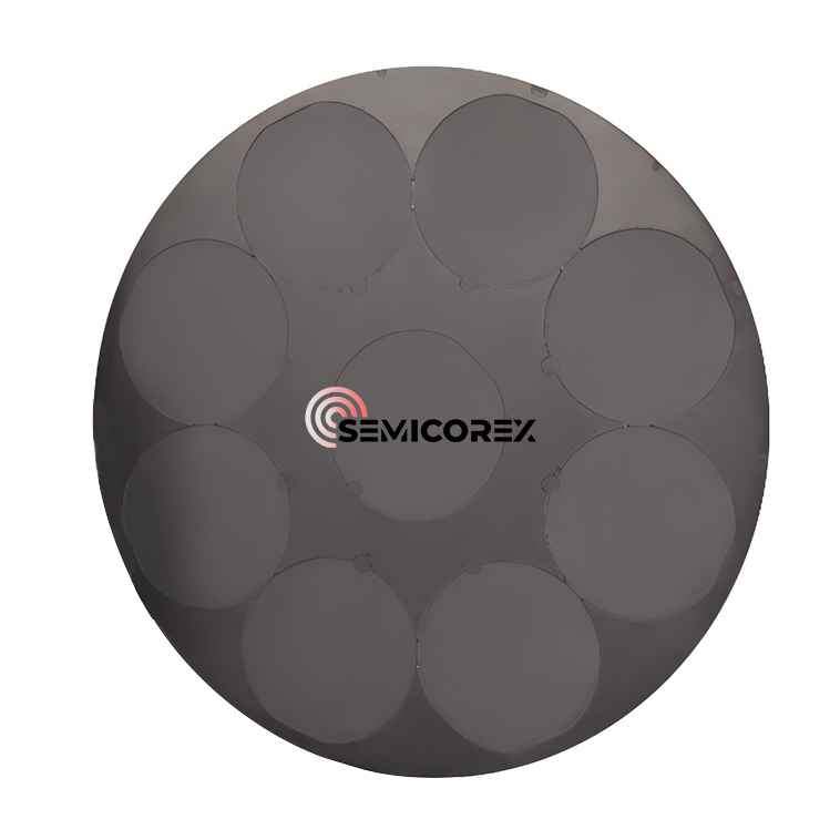
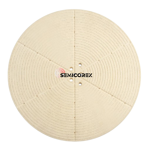
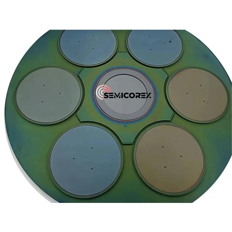
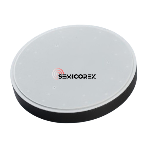
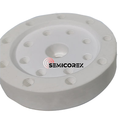
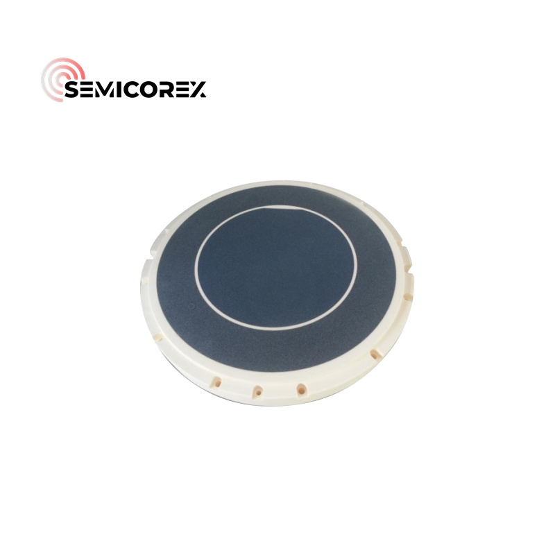
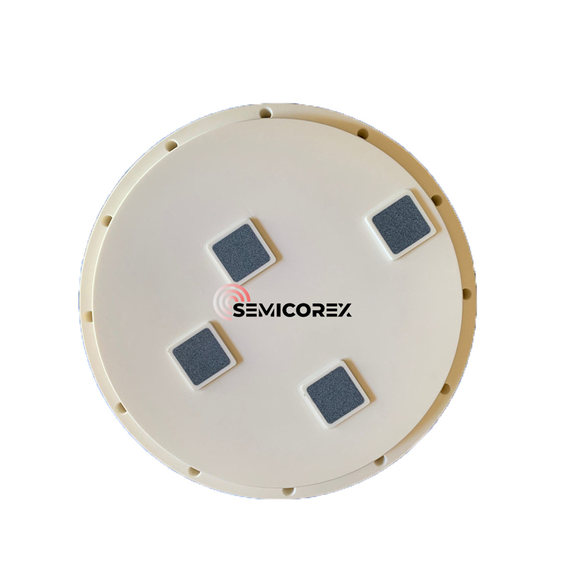
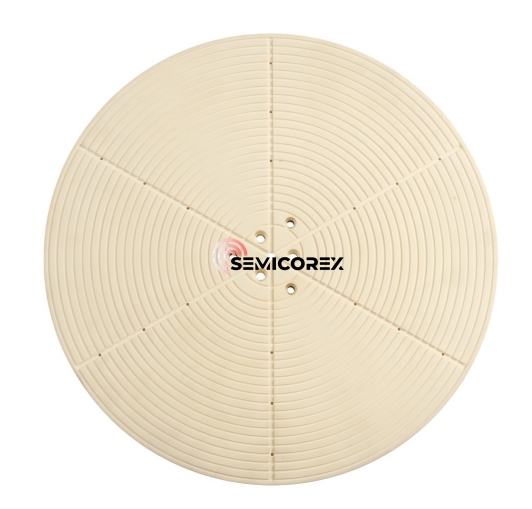
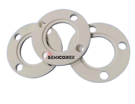
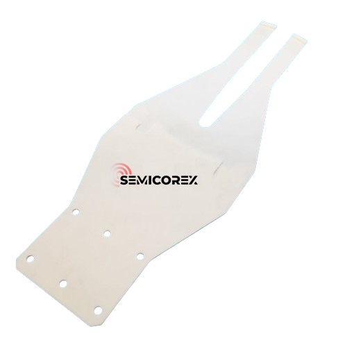
Semicorex ESC Chuck is a critical component in the semiconductor industry, specifically designed to securely hold wafers during various fabrication processes. Semicorex provides top-quality products at competitive prices, we are ready to become your long-term partner in China.*
Send Inquiry
Semicorex ESC Chuck utilizes electrostatic forces to maintain precise control over the wafer's position, ensuring high precision and repeatability in semiconductor manufacturing environments. The design of the ESC chuck, coupled with its robust material selection and customizable dimensions, makes it a versatile and essential tool in processes such as etching, deposition, and ion implantation.
ESC chuck works by applying a high-voltage electrostatic field between the chuck's electrodes and the wafer, creating an attractive force that holds the wafer in place. The wafer, typically made of silicon or silicon carbide, is secured by this force, allowing for precise operations in high-vacuum environments. This system eliminates the need for mechanical clamping or vacuum chucking, which can introduce contaminants or distort the wafer. By using an ESC chuck, manufacturers can achieve a cleaner, more stable environment for delicate fabrication processes, leading to higher yields and more consistent results.
One of the key advantages of ESC technology is its ability to maintain a firm grip on the wafer while distributing force evenly across its surface. This ensures that the wafer remains flat and stable, which is crucial for achieving uniform etching or deposition, especially in processes where submicron precision is required. The customizable dimensions of the ESC chuck allow it to accommodate wafers of different sizes, from standard 200mm and 300mm wafers to specialized, non-standard sizes used in research and development or in the production of niche semiconductor devices.
The materials used in the construction of the ESC chuck are carefully selected to ensure compatibility with the harsh environments typically found in semiconductor processing. High-purity ceramics alumina are used due to their excellent electrical insulating properties, thermal stability, and resistance to plasma corrosion. These properties allow the chuck to function effectively in both high-temperature and high-vacuum conditions, providing the durability and reliability required for long-term use in a cleanroom environment.
Customization is another significant benefit of ESC chucks. Depending on the specific requirements of a semiconductor fabrication process, the chuck’s dimensions, electrode configurations, and material compositions can be tailored to meet the unique needs of the equipment and wafers being processed. Whether the application involves plasma etching, chemical vapor deposition (CVD), or physical vapor deposition (PVD), the ESC chuck can be engineered to optimize performance and maintain the integrity of the wafer during processing.


