- English
- Español
- Português
- русский
- Français
- 日本語
- Deutsch
- tiếng Việt
- Italiano
- Nederlands
- ภาษาไทย
- Polski
- 한국어
- Svenska
- magyar
- Malay
- বাংলা ভাষার
- Dansk
- Suomi
- हिन्दी
- Pilipino
- Türkçe
- Gaeilge
- العربية
- Indonesia
- Norsk
- تمل
- český
- ελληνικά
- український
- Javanese
- فارسی
- தமிழ்
- తెలుగు
- नेपाली
- Burmese
- български
- ລາວ
- Latine
- Қазақша
- Euskal
- Azərbaycan
- Slovenský jazyk
- Македонски
- Lietuvos
- Eesti Keel
- Română
- Slovenski
- मराठी
- Srpski језик
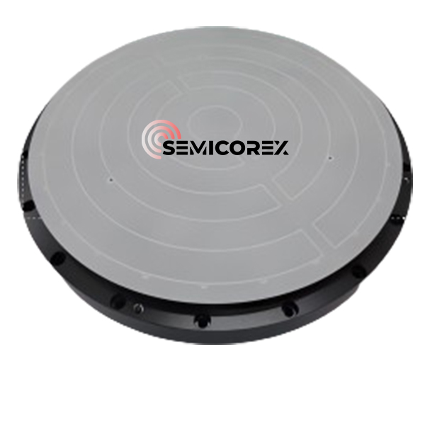
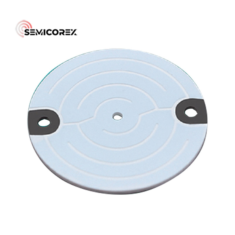
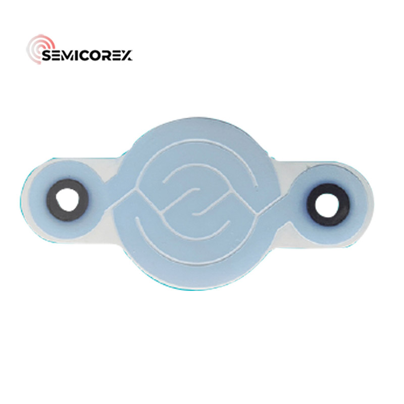
PBN Electrostatic Chuck
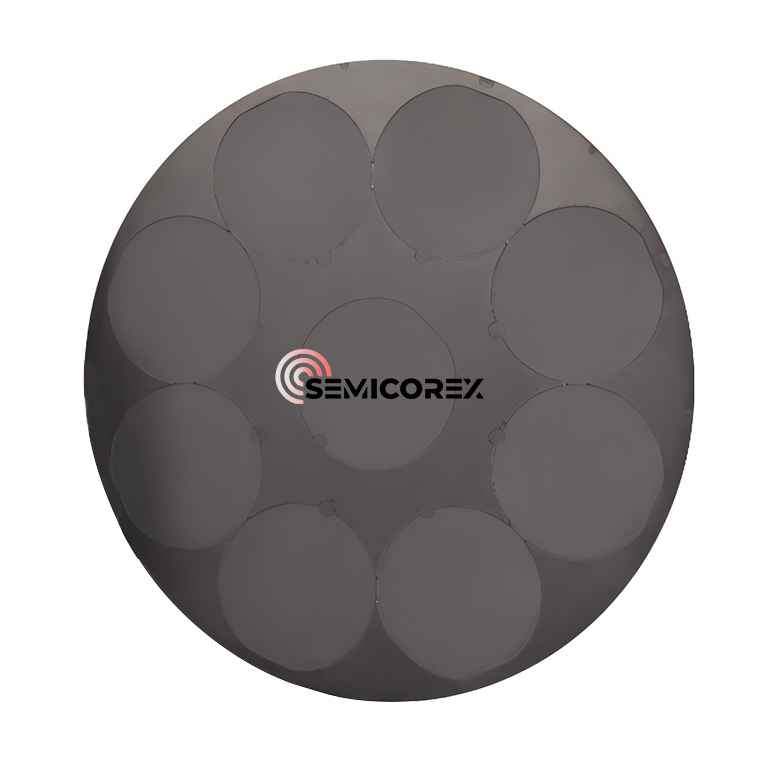
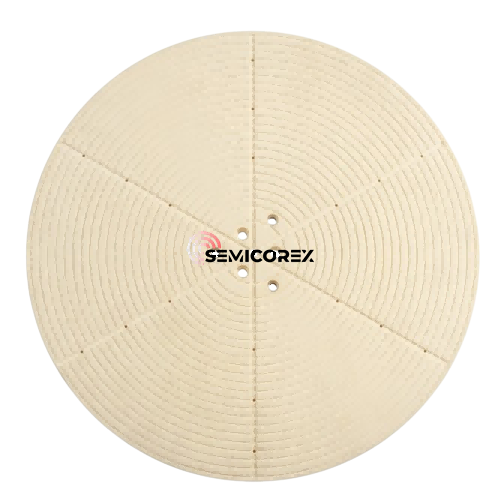
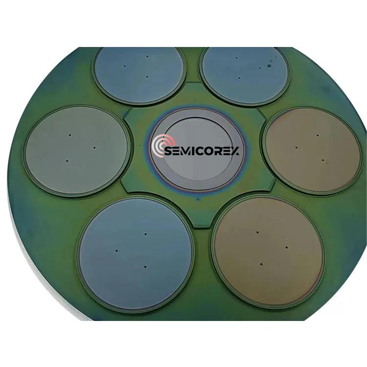
The PBN Electrostatic Chuck by Semicorex stands out in the field of wafer handling in semiconductor manufacturing due to its unique material properties.
Send Inquiry
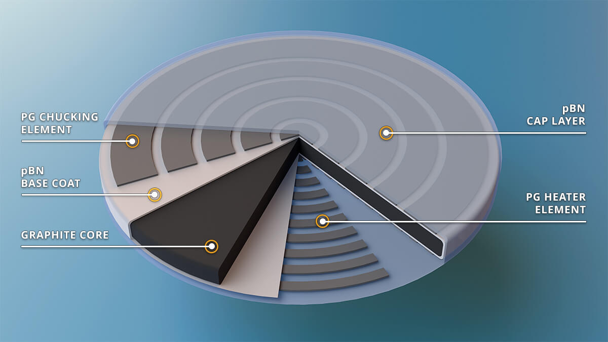 Material Properties of PBN Electrostatic Chuck
High-Temperature Resistance and Dielectric Strength
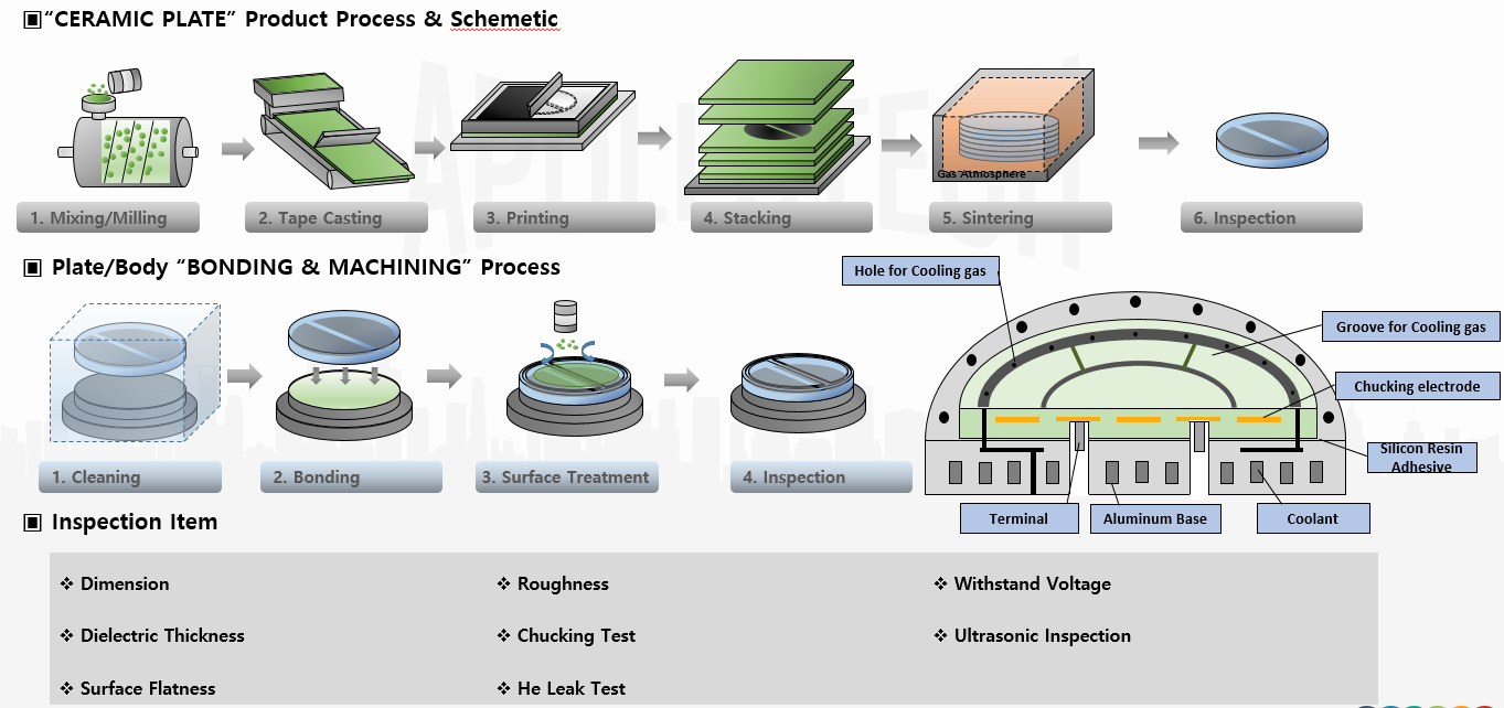
The PBN Electrostatic Chuck is renowned for its exceptional high-temperature resistance, a trait that is pivotal in the semiconductor manufacturing process. Pyrolytic Boron Nitride (PBN), the material used in the construction of the chuck, exhibits a resistivity higher than most commonly used ceramics, which is crucial for maintaining the Johnsen-Rahbek (J-R) chuck force up to temperatures of 1050°C. This high resistivity, coupled with its high dielectric strength, ensures that electrical breakdown is effectively prevented even under intense heat, thereby enhancing the operational reliability of the chuck.
Thermal Uniformity and Shock Resistance
PBN's hexagonal lattice structure, prepared through chemical vapor deposition at temperatures exceeding 1500°C, contributes to its outstanding thermal uniformity and shock resistance. The high-density heating elements within the PBN Electrostatic Chuck enable it to achieve a consistent wafer thermal profile with good uniformity of 1.1–1.5% at temperatures of 600–800°C. Moreover, the PBN-based chuck demonstrates remarkable thermal shock resistance and lower thermal mass, allowing it to reach 600°C at a rapid ramping speed of 23°C/sec without the risk of cracking or delamination.
Customizable Multi-Zone Heating
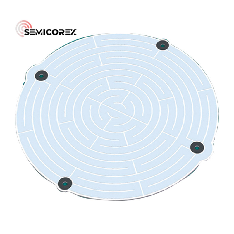
The PBN Electrostatic Chuck is highly customizable, featuring multi-zone heating capabilities that allow for maximum temperature control. This level of customization ensures that each chuck can be tailored to meet the specific requirements of individual customers, providing a flexible solution for various semiconductor processing applications.
Applications of PBN Electrostatic Chuck
Ion Implantation and Wafer Handling
The PBN Electrostatic Chuck is the preferred wafer-handling apparatus in ion implantation processes. Its ability to hold wafers at temperatures exceeding 1000°C makes it one of the most versatile electrostatic chucks on the market. This versatility is further enhanced by its capacity to maintain wafers within very tight temperature ranges, thanks to the high-density, multizone heating elements.
Silicon Carbide Ion Implantation
In the specific application of SiC ion implantation, the PBN Electrostatic Chuck offers a viable solution to the challenges of wafer heating and handling. Its dual-function capabilities, which include high chuck force, high heating power, good thermal uniformity, and fast response, make it an ideal choice for addressing the complex requirements of SiC ion implantation.
Semiconductor Manufacturing
The PBN Electrostatic Chuck plays a critical role in semiconductor manufacturing, where precise wafer handling and temperature control are essential. Its high thermal shock resistance and rapid temperature ramping capabilities make it suitable for advanced semiconductor processes that demand rigorous temperature management and rapid thermal cycling.

