- English
- Español
- Português
- русский
- Français
- 日本語
- Deutsch
- tiếng Việt
- Italiano
- Nederlands
- ภาษาไทย
- Polski
- 한국어
- Svenska
- magyar
- Malay
- বাংলা ভাষার
- Dansk
- Suomi
- हिन्दी
- Pilipino
- Türkçe
- Gaeilge
- العربية
- Indonesia
- Norsk
- تمل
- český
- ελληνικά
- український
- Javanese
- فارسی
- தமிழ்
- తెలుగు
- नेपाली
- Burmese
- български
- ລາວ
- Latine
- Қазақша
- Euskal
- Azərbaycan
- Slovenský jazyk
- Македонски
- Lietuvos
- Eesti Keel
- Română
- Slovenski
- मराठी
- Srpski језик
Company News
Demystifying Electrostatic Chuck (ESC) Technology in Wafer Handling
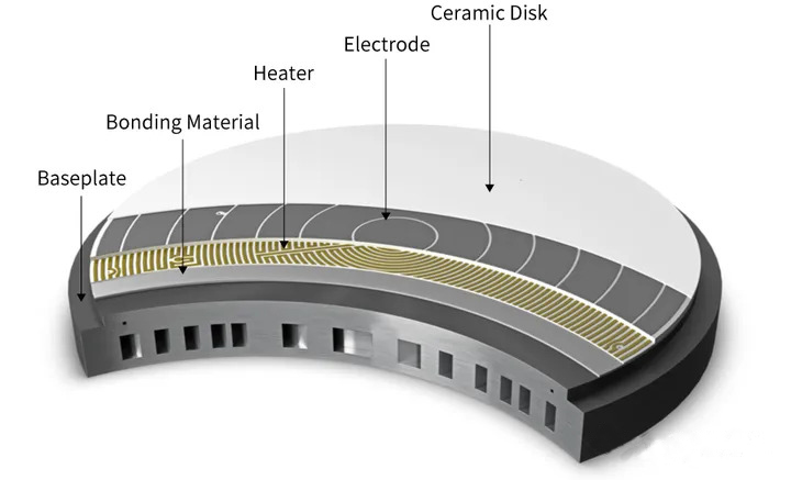
Electrostatic chucks (ESCs) have become indispensable in semiconductor manufacturing and flat panel display production, offering a damage-free, highly controllable method for holding and positioning delicate wafers and substrates during critical processing steps. This article delves into the intrica......
Read MoreHigh-Purity CVD Thick SiC: Process Insights for Material Growth
Thick, high-purity silicon carbide (SiC) layers, typically exceeding 1mm, are critical components in various high-value applications, including semiconductor fabrication and aerospace technologies. This article delves into the Chemical Vapor Deposition (CVD) process for producing such layers, highli......
Read MoreUnderstanding Chemical Vapor Deposition (CVD): A Comprehensive Overview
Chemical Vapor Deposition (CVD) is a versatile thin-film deposition technique widely employed in the semiconductor industry for fabricating high-quality, conformal thin films on various substrates. This process involves chemical reactions of gaseous precursors onto a heated substrate surface, result......
Read MoreSiC Boats vs. Quartz Boats: Current Usage and Future Trends in Semiconductor Manufacturing
This article delves into the usage and future trajectory of silicon carbide (SiC) boats in relation to quartz boats within the semiconductor industry, specifically focusing on their applications in solar cell manufacturing.
Read MoreGallium Nitride Epitaxial Wafers: An Introduction to the Fabrication Process
Gallium Nitride (GaN) epitaxial wafer growth is a complex process, often utilizing a two-step method. This method involves several critical stages, including high-temperature baking, buffer layer growth, recrystallization, and annealing. By meticulously controlling the temperature throughout these s......
Read More
