- English
- Español
- Português
- русский
- Français
- 日本語
- Deutsch
- tiếng Việt
- Italiano
- Nederlands
- ภาษาไทย
- Polski
- 한국어
- Svenska
- magyar
- Malay
- বাংলা ভাষার
- Dansk
- Suomi
- हिन्दी
- Pilipino
- Türkçe
- Gaeilge
- العربية
- Indonesia
- Norsk
- تمل
- český
- ελληνικά
- український
- Javanese
- فارسی
- தமிழ்
- తెలుగు
- नेपाली
- Burmese
- български
- ລາວ
- Latine
- Қазақша
- Euskal
- Azərbaycan
- Slovenský jazyk
- Македонски
- Lietuvos
- Eesti Keel
- Română
- Slovenski
- मराठी
- Srpski језик
The Fusion of AI and Physics: CVD Technological Innovation Behind the Nobel Prize
2024-12-05
The recent announcement of the 2024 Nobel Prize in Physics has brought unprecedented attention to the field of artificial intelligence. The research conducted by American scientist John J. Hopfield and Canadian scientist Geoffrey E. Hinton has utilized machine learning tools to provide new insights into the complex world of physics today. This achievement not only marks an important milestone in AI technology but also heralds a deep integration between physics and artificial intelligence.
What is the Significance of Chemical Vapor Deposition (CVD) in Physics and What Challenges Does it Face?
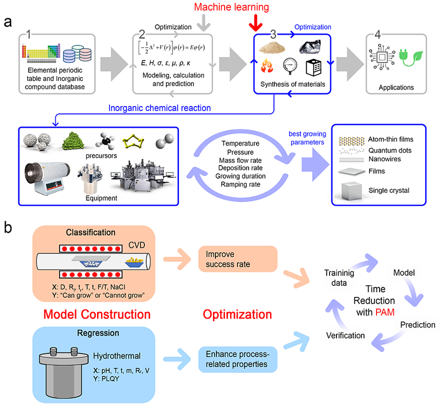
Chemical vapor deposition (CVD) technology holds multifaceted significance in physics, serving as a crucial material preparation technique while playing an essential role in advancing research and applications in the physical sciences. CVD enables precise control over material growth at atomic and molecular levels. As illustrated in Figure 1, this technique involves gaseous or vapor-phase substances undergoing chemical reactions on solid surfaces to form solid deposits, thereby producing a variety of high-performance films and nanostructured materials. This capability is vital in physics for understanding and exploring the relationship between materials’ microstructures and their macroscopic properties, as it allows scientists to study materials with specific structures and compositions, thereby gaining in-depth insights into their physical properties.
Furthermore, CVD technology is a key method for producing various functional films in semiconductor devices. For instance, it can be used to grow silicon single-crystal epitaxial layers, III-V semiconductors like gallium arsenide, and II-VI semiconductor single-crystal epi-layers, as well as deposit various doped semiconductor single-crystal epitaxial films and polysilicon films. These materials and structures form the foundation of modern electronic and optoelectronic devices. Additionally, CVD technology plays a significant role in research fields such as optical materials, superconducting materials, and magnetic materials. By using CVD, thin films with specific optical properties can be synthesized for applications in optoelectronic devices and optical sensors.
Despite its advantages, CVD technology faces several challenges in practical applications, such as:
High-temperature and high-pressure conditions: CVD often requires high temperatures or pressures, limiting the types of materials that can be used and increasing energy consumption and costs.
Sensitivity to parameters: The CVD process is extremely sensitive to reaction conditions, with even slight variations potentially affecting the quality of the final product.
Complexity of CVD systems: The process is sensitive to boundary conditions, exhibits significant uncertainty, and can be difficult to control reproducibly, potentially complicating material development.
How Does Chemical Vapor Deposition (CVD) Technology Benefit from Machine Learning?
Confronted with these challenges, machine learning, as a powerful data analysis tool, has shown potential in addressing some of these issues within the CVD field. Here are cases of machine learning applications in CVD technology:
(1) Predicting CVD Growth: Machine learning algorithms can learn from extensive experimental data to predict CVD growth outcomes under various conditions, thereby guiding the adjustment of experimental parameters. As depicted in Figure 1, a research team at Nanyang Technological University in Singapore used classification algorithms in machine learning to guide the CVD synthesis of two-dimensional materials. By analyzing early experimental data, they successfully predicted the growth conditions for molybdenum disulfide (MoS2), significantly improving the success rate of experiments and reducing the number of trials.

Figure 1: Machine Learning-Guided Material Synthesis. (a) An indispensable part of material development: material synthesis. (b) Classification models facilitate the chemical vapor deposition (CVD) synthesis of two-dimensional materials (top); regression models guide the hydrothermal synthesis of sulfur and nitrogen-doped fluorescent quantum dots (bottom).
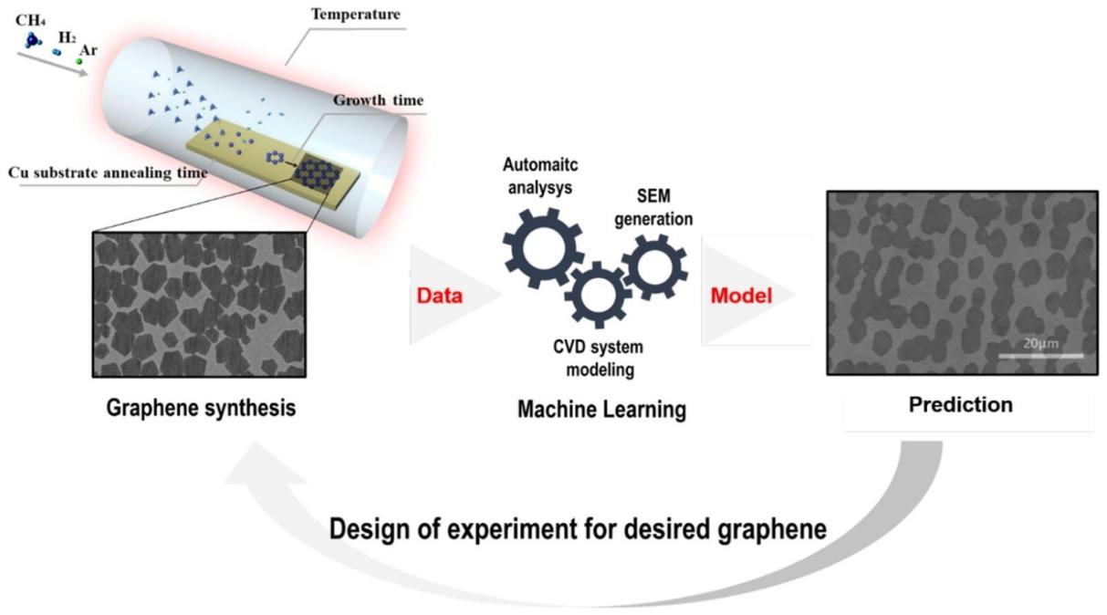
In another study, as depicted in Figure 2, machine learning was employed to analyze graphene growth patterns within CVD systems. By developing region proposal convolutional neural networks (R-CNN), researchers were able to automatically measure and analyze the size, coverage, domain density, and aspect ratio of graphene. Subsequently, artificial neural networks (ANN) and support vector machines (SVM) were used to develop surrogate models to deduce the correlation between CVD process variables and measured specifications. This method enables the simulation of graphene synthesis and determines the experimental conditions necessary for producing graphene with large grain sizes and low domain density, thereby saving significant time and costs.

Figure 2: Machine Learning Prediction of Graphene Growth Patterns in CVD Systems
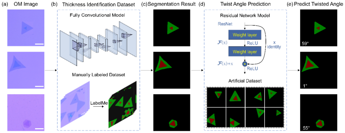
(2) Automated CVD Process: Machine learning can be used to develop automated systems that monitor and adjust parameters in real-time during the CVD process, achieving more precise control and higher production efficiency. As shown in Figure 3, a research team from Xidian University utilized deep learning to overcome the challenge of recognizing the rotation angle of bilayer two-dimensional materials prepared by CVD. By collecting the color space of CVD-prepared MoS2 and applying semantic segmentation convolutional neural networks (CNN), they were able to accurately and quickly identify the thickness of MoS2. They then trained a second CNN model to precisely predict the rotation angle of bilayer TMD materials grown by CVD. This method not only improved sample identification efficiency but also provided a new paradigm for the application of deep learning in the field of materials science.

Figure 3: Deep Learning Approach for Identifying the Rotation Angle of Bilayer Two-Dimensional Materials
Outlook
The announcement of the Nobel Prize once again reminds us that the integration of artificial intelligence and physics will bring about more innovation and breakthroughs. As machine learning technology continues to advance, we have reason to believe that chemical vapor deposition technology will encounter new development opportunities in the future. All of this heralds the dawn of a new era, where the convergence of technology and science will open up broader avenues for exploration.
Semicorex offers SiC/TaC coating graphite and ceramic materials through the chemical vapor deposition(CVD) process. If you have any inquiries or need additional details, please don't hesitate to get in touch with us.
Contact phone # +86-13567891907
Email: sales@semicorex.com


