- English
- Español
- Português
- русский
- Français
- 日本語
- Deutsch
- tiếng Việt
- Italiano
- Nederlands
- ภาษาไทย
- Polski
- 한국어
- Svenska
- magyar
- Malay
- বাংলা ভাষার
- Dansk
- Suomi
- हिन्दी
- Pilipino
- Türkçe
- Gaeilge
- العربية
- Indonesia
- Norsk
- تمل
- český
- ελληνικά
- український
- Javanese
- فارسی
- தமிழ்
- తెలుగు
- नेपाली
- Burmese
- български
- ລາວ
- Latine
- Қазақша
- Euskal
- Azərbaycan
- Slovenský jazyk
- Македонски
- Lietuvos
- Eesti Keel
- Română
- Slovenski
- मराठी
- Srpski језик
Etching Process Parameters
2024-12-05
Etching is a critical step in chip manufacturing, used to create minute circuit structures on silicon wafers. It involves the removal of material layers through chemical or physical means to meet specific design requirements. This article will introduce several key etching parameters, including incomplete etching, over-etching, etch rate, undercutting, selectivity, uniformity, aspect ratio, and isotropic/anisotropic etching.
What is Incomplete Etching?
Incomplete etching occurs when the material in the designated area is not entirely removed during the etching process, leaving residual layers in patterned holes or on surfaces. This situation can arise from various factors, such as insufficient etching time or uneven film thickness.
Over-Etching
To ensure complete removal of all necessary material and account for variations in surface layer thickness, a certain amount of over-etching is typically incorporated into the design. This means the actual etching depth exceeds the target value. Appropriate over-etching is essential for the successful execution of subsequent processes.
Etch Rate
The etch rate refers to the thickness of material removed per unit time and is a crucial indicator of etching efficiency. A common phenomenon is the loading effect, where insufficient reactive plasma leads to reduced etch rates or uneven etch distribution. This can be improved by adjusting process conditions such as pressure and power.

Undercutting
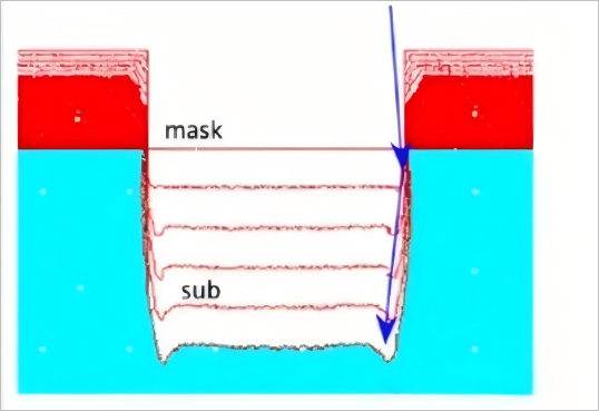
Undercutting occurs when etching not only happens in the target area but also extends downward along the edges of the photoresist. This phenomenon can cause inclined sidewalls, affecting device dimensional accuracy. Controlling gas flow and etching time helps reduce the occurrence of undercutting.

Selectivity
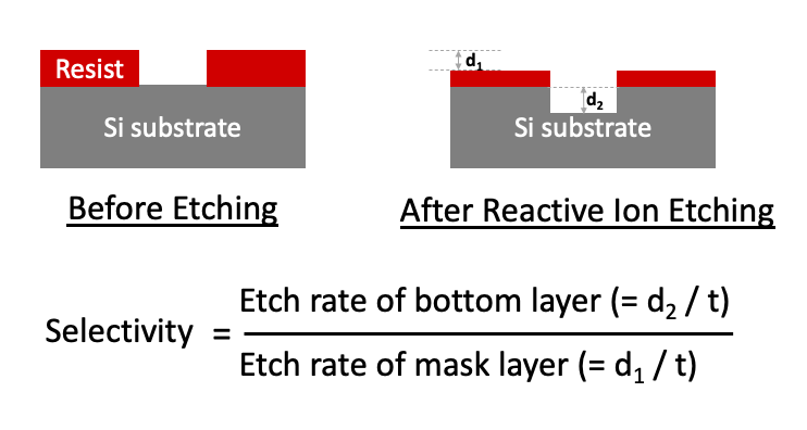
Selectivity is the ratio of etch rates between two different materials under the same conditions. A high selectivity enables more precise control over which parts are etched and which are retained, which is crucial for creating complex multilayer structures.

Uniformity
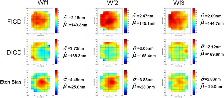
Uniformity measures the consistency of etching effects across an entire wafer or between batches. Good uniformity ensures that each chip has similar electrical characteristics.

Aspect Ratio
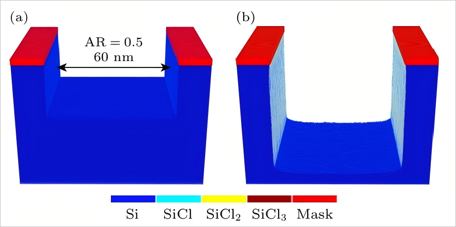
Aspect ratio is defined as the ratio of feature height to width. As technology evolves, there is an increasing demand for higher aspect ratios to make devices more compact and efficient. However, this presents challenges for etching, as it requires maintaining verticality while avoiding excessive erosion at the bottom.
How Do Isotropic and Anisotropic Etching Differ?
Isotropic etching occurs uniformly in all directions and is suitable for certain specific applications. In contrast, anisotropic etching primarily progresses in the vertical direction, making it ideal for creating precise three-dimensional structures. Modern integrated circuit manufacturing often favors the latter for better shape control.
Semicorex offers high-quality SiC/TaC solutions for semiconductor ICP/PSS etching and Plasma etching process. If you have any inquiries or need additional details, please don't hesitate to get in touch with us.
Contact phone # +86-13567891907
Email: sales@semicorex.com


