- English
- Español
- Português
- русский
- Français
- 日本語
- Deutsch
- tiếng Việt
- Italiano
- Nederlands
- ภาษาไทย
- Polski
- 한국어
- Svenska
- magyar
- Malay
- বাংলা ভাষার
- Dansk
- Suomi
- हिन्दी
- Pilipino
- Türkçe
- Gaeilge
- العربية
- Indonesia
- Norsk
- تمل
- český
- ελληνικά
- український
- Javanese
- فارسی
- தமிழ்
- తెలుగు
- नेपाली
- Burmese
- български
- ລາວ
- Latine
- Қазақша
- Euskal
- Azərbaycan
- Slovenský jazyk
- Македонски
- Lietuvos
- Eesti Keel
- Română
- Slovenski
- मराठी
- Srpski језик
Semiconductor doping process
2024-12-03
One of the unique properties of semiconductor materials is that their conductivity, as well as their conductivity type (N-type or P-type), can be created and controlled through a process called doping. This involves introducing specialized impurities, known as dopants, into the material to form junctions on the surface of the wafer. The industry employs two main doping techniques: thermal diffusion and ion implantation.
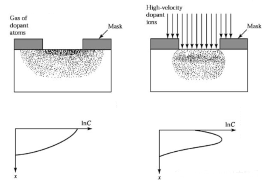
In thermal diffusion, dopant materials are introduced into the exposed surface of the top layer of the wafer, typically using openings in the silicon dioxide layer. By applying heat, these dopants diffuse into the body of the wafer. The amount and depth of this diffusion are regulated by specific rules derived from chemical principles, which dictate how dopants move within the wafer at elevated temperatures.
In contrast, ion implantation involves injecting dopant materials directly into the surface of the wafer. Most of the dopant atoms that are introduced remain stationary below the surface layer. Similar to thermal diffusion, the movement of these implanted atoms is also controlled by diffusion rules. Ion implantation has largely replaced the older thermal diffusion technique and is now essential in the production of smaller and more complex devices.

Common Doping Processes and Applications
1.Diffusion Doping: In this method, impurity atoms are diffused into a silicon wafer using a high-temperature diffusion furnace, which forms a diffusion layer. This technique is primarily used in the manufacture of large-scale integrated circuits and microprocessors.
2.Ion Implantation Doping: This process involves directly injecting impurity ions into the silicon wafer with an ion implanter, creating an ion implantation layer. It allows for high doping concentration and precise control, making it suitable for the production of high-integration and high-performance chips.
3. Chemical Vapor Deposition Doping: In this technique, a doped film, such as silicon nitride, is formed on the surface of the silicon wafer through chemical vapor deposition. This method offers excellent uniformity and repeatability, making it ideal for manufacturing specialized chips.
4. Epitaxial Doping: This approach involves growing a doped single crystal layer, such as phosphorus-doped silicon glass, epitaxially on a single crystal substrate. It is particularly suitable for crafting high-sensitivity and high-stability sensors.
5. Solution Method: The solution method allows for varying doping concentrations by controlling the composition of the solution and the immersion time. This technique is applicable to many materials, especially those with porous structures.
6. Vapor Deposition Method: This method involves forming new compounds by reacting external atoms or molecules with those on the surface of the material, thus controlling the doping materials. It is particularly suited for doping thin films and nanomaterials.
Each type of doping process has its unique characteristics and range of applications. In practical uses, it is important to select the appropriate doping process based on specific needs and material properties to achieve optimal doping results.
Doping technology has a broad range of applications across various fields:
- Semiconductor Manufacturing: Doping is a core technology in semiconductor manufacturing, primarily used to create transistors, integrated circuits, solar cells, and more. The doping process modifies the conductivity and optoelectronic properties of semiconductors, enabling devices to meet specific functional and performance requirements.
- Electronic Packaging: In electronic packaging, doping technology is utilized to enhance the thermal conductivity and electrical properties of packaging materials. This process improves both the heat dissipation performance and the reliability of electronic devices.
- Chemical Sensors: Doping is widely applied in the field of chemical sensors for the production of sensitive membranes and electrodes. By altering the sensitivity and response speed of sensors, doping facilitates the development of devices that boast high sensitivity, selectivity, and rapid response times.
- Biosensors: Similarly, in the domain of biosensors, doping technology is employed to manufacture biochips and biosensors. This process modifies the electrical properties and biological characteristics of biomaterials, leading to biosensors that are highly sensitive, specific, and cost-effective.
- Other Fields: Doping technology is also used in various materials, including magnetic, ceramic, and glass materials. Through doping, the magnetic, mechanical, and optical properties of these materials can be altered, resulting in high-performance materials and devices.
As a crucial material modification technique, doping technology is integral to multiple fields. Continuously enhancing and refining the doping process is essential for achieving high-performance materials and devices.
Semicorex offers high-quality SiC solutions for semiconductor diffusion process. If you have any inquiries or need additional details, please don't hesitate to get in touch with us.
Contact phone # +86-13567891907
Email: sales@semicorex.com


