- English
- Español
- Português
- русский
- Français
- 日本語
- Deutsch
- tiếng Việt
- Italiano
- Nederlands
- ภาษาไทย
- Polski
- 한국어
- Svenska
- magyar
- Malay
- বাংলা ভাষার
- Dansk
- Suomi
- हिन्दी
- Pilipino
- Türkçe
- Gaeilge
- العربية
- Indonesia
- Norsk
- تمل
- český
- ελληνικά
- український
- Javanese
- فارسی
- தமிழ்
- తెలుగు
- नेपाली
- Burmese
- български
- ລາວ
- Latine
- Қазақша
- Euskal
- Azərbaycan
- Slovenský jazyk
- Македонски
- Lietuvos
- Eesti Keel
- Română
- Slovenski
- मराठी
- Srpski језик

GaN Single Crystal
Semiconductor technology has been the backbone of modern civilization, fundamentally transforming the way we live, work, and interact with the world. It has enabled unprecedented advancements in various fields including information technology, energy, telecommunications, and healthcare. From the microprocessors that power our smartphones and computers, to the sensors in medical devices, and the power electronics in renewable energy systems, semiconductors are at the core of nearly every technological innovation of the past century.
First Generation of Semiconductors: Germanium and Silicon
The history of semiconductor technology began with the first generation of semiconductors, primarily germanium (Ge) and silicon (Si). These materials are elemental semiconductors, meaning they are composed of a single element. Silicon, in particular, has been the most widely used semiconductor material due to its abundance, cost-effectiveness, and excellent electronic properties. Silicon-based technology has matured over decades, leading to the development of integrated circuits (ICs) that form the foundation of modern electronics. Silicon’s ability to form a stable and high-quality oxide layer (silicon dioxide) has been a critical factor in the success of metal-oxide-semiconductor (MOS) devices, which are the building blocks of most digital electronics.
Second Generation of Semiconductors: Gallium Arsenide and Indium Phosphide
As technology evolved, the limitations of silicon became apparent, particularly in high-speed and high-frequency applications. This led to the development of the second generation of semiconductors, which includes compound semiconductors like gallium arsenide (GaAs) and indium phosphide (InP). These materials are known for their superior electron mobility and direct bandgap, making them ideal for optoelectronic devices such as light-emitting diodes (LEDs), laser diodes, and high-frequency transistors. GaAs, for instance, is widely used in microwave and millimeter-wave communication systems, as well as in satellite and radar technologies. Despite their advantages, the widespread adoption of GaAs and InP has been limited due to higher costs and challenges in manufacturing.
Third Generation of Semiconductors: Silicon Carbide and Gallium Nitride
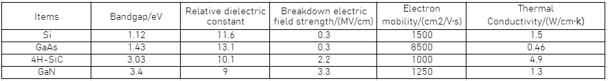
In recent years, the focus has shifted to the third generation of semiconductors, which includes materials like silicon carbide (SiC) and gallium nitride (GaN). These materials possess a wide bandgap, meaning they can operate at higher voltages, temperatures, and frequencies than their predecessors. GaN, in particular, has garnered significant attention for its exceptional properties, including a wide bandgap of 3.4 eV, high electron mobility, high breakdown voltage, and excellent thermal conductivity. These characteristics make GaN an ideal candidate for high-power and high-frequency applications, such as fast chargers, power transistors, and radio-frequency (RF) microwave devices.
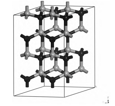
Crystal Structure and Bonding in GaN
GaN belongs to the III-V group of compound semiconductors, which are composed of elements from group III (e.g., gallium) and group V (e.g., nitrogen) of the periodic table. The crystal structure of GaN can exist in two primary forms: hexagonal wurtzite and cubic sphalerite. The type of crystal structure that forms is influenced by the nature of the chemical bonds between the atoms. In semiconductor compounds, the bonding can be a mix of covalent and ionic bonds. The more ionic the bond, the more likely the material is to form a wurtzite structure. In the case of GaN, the large difference in electronegativity between gallium (Ga) and nitrogen (N) leads to a significant ionic character in the bond. As a result, GaN typically crystallizes in the wurtzite structure, which is known for its high thermal stability and resistance to chemical corrosion.
Advantages of GaN Over Earlier Semiconductor Materials
Compared to first and second-generation semiconductor materials, GaN offers several advantages that make it particularly attractive for cutting-edge applications. One of the most significant benefits is its wide bandgap, allowing GaN-based devices to operate at higher voltages and temperatures without breaking down. This makes GaN an excellent material for power electronics, where efficiency and thermal management are critical concerns. Additionally, GaN has a lower dielectric constant, helping to reduce capacitance and enable faster switching speeds in transistors.
GaN also boasts a higher critical electric field strength, allowing devices to handle larger electric fields without experiencing a breakdown. This is particularly important in high-power applications, where the ability to manage high voltages and currents is essential. Furthermore, GaN’s high electron mobility contributes to its suitability for high-frequency applications, such as RF and microwave devices. The combination of these properties—high thermal conductivity, high temperature resistance, and radiation hardness—makes GaN a versatile material that is poised to play a crucial role in the next generation of electronic devices.
GaN in Modern Applications and Future Prospects
The unique properties of GaN have already begun to revolutionize several industries. In consumer electronics, GaN-based fast chargers are becoming increasingly popular due to their efficiency and compact size compared to traditional silicon-based chargers. In the realm of telecommunications, GaN is being used to develop high-frequency transistors that are essential for 5G networks and beyond. The aerospace and defense sectors are also exploring GaN’s potential for use in high-power radar and communication systems, where its ability to operate under extreme conditions is invaluable.