
- English
- Español
- Português
- русский
- Français
- 日本語
- Deutsch
- tiếng Việt
- Italiano
- Nederlands
- ภาษาไทย
- Polski
- 한국어
- Svenska
- magyar
- Malay
- বাংলা ভাষার
- Dansk
- Suomi
- हिन्दी
- Pilipino
- Türkçe
- Gaeilge
- العربية
- Indonesia
- Norsk
- تمل
- český
- ελληνικά
- український
- Javanese
- فارسی
- தமிழ்
- తెలుగు
- नेपाली
- Burmese
- български
- ລາວ
- Latine
- Қазақша
- Euskal
- Azərbaycan
- Slovenský jazyk
- Македонски
- Lietuvos
- Eesti Keel
- Română
- Slovenski
- मराठी
- Srpski језик

Method of GaN Crystal Growth
When producing large-sized GaN single crystal substrates, HVPE is currently the best choice for commercialization. However, the back carrier concentration of the grown GaN cannot be precisely controlled. MOCVD is the most mature growth method at present, but it faces challenges such as expensive raw materials. The ammonothermal method for growing GaN offers stable and balanced growth and high crystal quality, but its growth rate is too slow for large-scale commercial growth. The solvent method cannot be precisely control the nucleation process, but it has low dislocation density and great potential for future development. Other methods, such as atomic layer deposition and magnetron sputtering, also come with their own advantages and disadvantages.
HVPE method
HVPE is called Hydride Vapor Phase Epitaxy. It has the advantages of fast growth rate and large-size crystals. It is not only one of the most mature technologies in the current process, but also the main method for commercially providing GaN single crystal substrates. In 1992, Detchprohm et al. first used HVPE to grow GaN thin films (400 nm), and the HVPE method has received widespread attention.
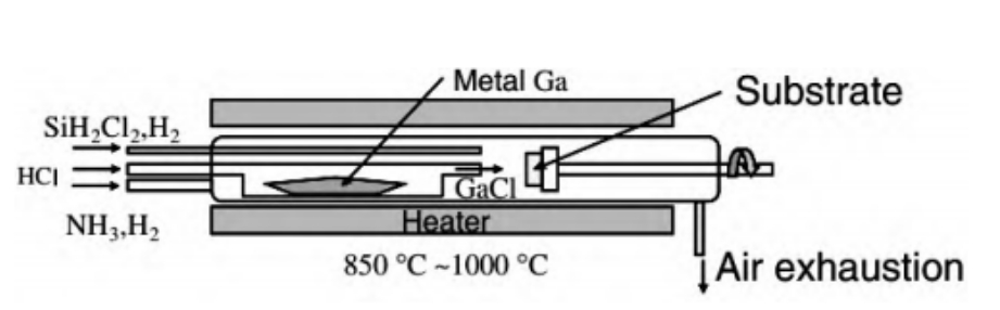
First, in the source area, HCl gas reacts with liquid Ga to generate gallium source (GaCl3), and the product is transported to the deposition area together with N2 and H2. In the deposition area, Ga source and N source (gaseous NH3) react to generate GaN (solid) when the temperature reaches 1000 °C. Generally, the factors affecting the growth rate of GaN are HCl gas and NH3. Nowadays, the purpose of stable growth of GaN can be achieved by improving and optimizing HVPE equipment and improving growth conditions.
The HVPE method is mature and has a fast growth rate, but it has the disadvantages of low quality yield of grown crystals and poor product consistency. Due to technical reasons, companies on the market generally adopt heteroepitaxial growth. Heteroepitaxial growth is generally done by separating GaN into a single crystal substrate using separation technology such as thermal decomposition, laser lift-off, or chemical etching after growth on sapphire or Si.
MOCVD method
MOCVD is called metal organic compound vapor deposition. It has the advantages of stable growth rate and good growth quality, suitable for large-scale production. It is the most mature technology at present and has become one of the most widely used technologies in production. MOCVD was first proposed by Mannacevit scholars in the 1960s. In the 1980s, the technology became mature and perfect.
The growth of GaN single crystal materials in MOCVD mainly uses trimethylgallium (TMGa) or triethylgallium (TEGa) as gallium source. Both are liquid at room temperature. Considering factors such as melting point, most of the current market uses TMGa as gallium source, NH3 as reaction gas, and high-purity N2 as carrier gas. Under high temperature (600~1300 ℃) conditions, thin-layer GaN is successfully prepared on sapphire substrates.
The MOCVD method for growing GaN has excellent product quality, short growth cycle and high yield, but it has the disadvantages of expensive raw materials and the need for precise control of the reaction process.
Previous:GaN Single Crystal


