- English
- Español
- Português
- русский
- Français
- 日本語
- Deutsch
- tiếng Việt
- Italiano
- Nederlands
- ภาษาไทย
- Polski
- 한국어
- Svenska
- magyar
- Malay
- বাংলা ভাষার
- Dansk
- Suomi
- हिन्दी
- Pilipino
- Türkçe
- Gaeilge
- العربية
- Indonesia
- Norsk
- تمل
- český
- ελληνικά
- український
- Javanese
- فارسی
- தமிழ்
- తెలుగు
- नेपाली
- Burmese
- български
- ລາວ
- Latine
- Қазақша
- Euskal
- Azərbaycan
- Slovenský jazyk
- Македонски
- Lietuvos
- Eesti Keel
- Română
- Slovenski
- मराठी
- Srpski језик

SiC Ceramics: The Indispensable Material for High-Precision Components in Semiconductor Manufacturing
2024-08-08
SiC possesses a unique combination of desirable properties, including high density, high thermal conductivity, high bending strength, high modulus of elasticity, strong corrosion resistance, and excellent high-temperature stability. Its resistance to bending stress deformation and thermal strain makes it exceptionally well-suited for the harsh, corrosive, and ultra-high-temperature environments encountered in critical manufacturing processes like wafer epitaxy and etching. Consequently, SiC has found widespread applications in various semiconductor manufacturing stages, including grinding and polishing, thermal processing (annealing, oxidation, diffusion), lithography, deposition, etching, and ion implantation.
1. Grinding and Polishing: SiC Grinding Susceptors
After ingot slicing, wafers often exhibit sharp edges, burrs, chipping, micro-cracks, and other imperfections. To prevent these defects from compromising wafer strength, surface quality, and subsequent processing steps, a grinding process is employed. Grinding smooths the wafer edges, reduces thickness variations, improves surface parallelism, and removes damage caused by the slicing process. Double-sided grinding using grinding plates is the most common method, with ongoing advancements in plate material, grinding pressure, and rotational speed constantly improving wafer quality.
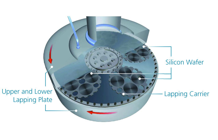
Double-Sided Grinding Mechanism
Traditionally, grinding plates were primarily made of cast iron or carbon steel. However, these materials suffer from short lifespans, high thermal expansion coefficients, and susceptibility to wear and thermal deformation, particularly during high-speed grinding or polishing, making it challenging to achieve consistent wafer flatness and parallelism. The advent of SiC ceramic grinding plates, with their exceptional hardness, low wear rate, and thermal expansion coefficient closely matching silicon, has led to the gradual replacement of cast iron and carbon steel. These properties make SiC grinding plates particularly advantageous for high-speed grinding and polishing processes.
2. Thermal Processing: SiC Wafers Carriers and Reaction Chamber Components
Thermal processing steps like oxidation, diffusion, annealing, and alloying are integral to wafer fabrication. SiC ceramic components are crucial in these processes, primarily as wafer carriers for transport between processing steps and as components within the reaction chambers of thermal processing equipment.
(1) Ceramic End Effectors(Arms):
During silicon wafer production, high-temperature processing is often required. Mechanical arms equipped with specialized end effectors are commonly used for transporting, handling, and positioning semiconductor wafers. These arms must operate in cleanroom environments, often under vacuum, high temperatures, and corrosive gas ambients, demanding high mechanical strength, corrosion resistance, high-temperature stability, wear resistance, hardness, and electrical insulation. While more expensive and challenging to manufacture, SiC ceramic arms outperform alumina alternatives in meeting these stringent requirements.
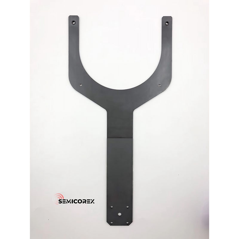
Semicorex SiC Ceramic End Effector
(2) Reaction Chamber Components:
Thermal processing equipment, such as oxidation furnaces (horizontal and vertical) and Rapid Thermal Processing (RTP) systems, operate at elevated temperatures, necessitating high-performance materials for their internal components. High-purity sintered SiC components, with their superior strength, hardness, modulus of elasticity, stiffness, thermal conductivity, and low thermal expansion coefficient, are indispensable for constructing the reaction chambers of these systems. Key components include vertical boats, pedestals, liner tubes, inner tubes, and baffle plates.
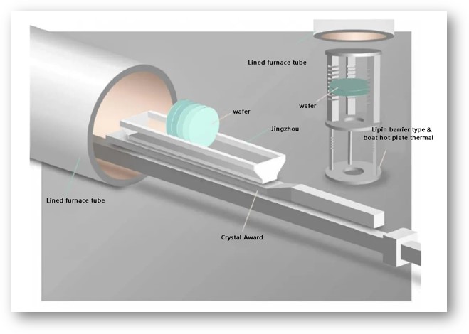
Reaction Chamber Components
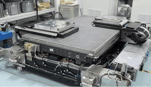
3. Lithography: SiC Stages and Ceramic Mirrors
Lithography, a critical step in semiconductor manufacturing, uses an optical system to focus and project light onto the wafer surface, transferring circuit patterns for subsequent etching. The precision of this process directly dictates the performance and yield of integrated circuits. As one of the most sophisticated pieces of equipment in chip manufacturing, a lithography machine comprises hundreds of thousands of components. To guarantee circuit performance and precision, stringent requirements are placed on the accuracy of both the optical elements and mechanical components within the lithography system. SiC ceramics play a vital role in this area, primarily in wafer stages and ceramic mirrors.
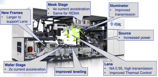
Lithography System Architecture
(1) Wafer Stages:
Lithography stages are responsible for holding the wafer and performing precise movements during exposure. Before each exposure, the wafer and stage must be aligned with nanometer precision, followed by alignment between the photomask and stage to ensure accurate pattern transfer. This requires high-speed, smooth, and highly precise automated control of the stage with nanometer-level accuracy. To meet these demands, lithography stages often utilize lightweight SiC ceramics with exceptional dimensional stability, low thermal expansion coefficients, and resistance to deformation. This minimizes inertia, reduces motor load, and enhances motion efficiency, positioning accuracy, and stability.
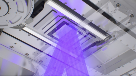
(2) Ceramic Mirrors:
Synchronized motion control between the wafer stage and reticle stage is crucial in lithography, directly impacting the overall accuracy and yield of the process. Stage mirrors are integral components of the stage scanning and positioning feedback measurement system. This system uses interferometers to emit measurement beams that reflect off the stage mirrors. By analyzing the reflected beams using the Doppler principle, the system calculates the stage’s position changes in real-time, providing feedback to the motion control system to ensure precise synchronization between the wafer stage and reticle stage. While lightweight SiC ceramics are suitable for this application, manufacturing such complex components presents significant challenges. Currently, mainstream integrated circuit equipment manufacturers primarily utilize glass ceramics or cordierite for this purpose. However, with advancements in material science and manufacturing techniques, researchers at the China Building Materials Academy have successfully fabricated large-size, complex-shaped, lightweight, fully enclosed SiC ceramic mirrors and other structural-functional optical components for lithography applications.
(3) Photomask Thin Films:
Photomasks, also known as reticles, are used to selectively transmit light and create patterns on photosensitive materials. However, EUV light irradiation can cause significant heating of the photomask, potentially reaching temperatures between 600 and 1000 degrees Celsius, leading to thermal damage. To mitigate this, a SiC thin film is often deposited on the photomask to enhance its thermal stability and prevent degradation.
4. Plasma Etching and Deposition: Focus Rings and Other Components
In semiconductor manufacturing, etching processes utilize plasmas generated from ionized gases (e.g., fluorine-containing gases) to selectively remove unwanted material from the wafer surface, leaving behind the desired circuit patterns. Thin film deposition, conversely, involves depositing insulating materials between metal layers to form dielectric layers, similar to a reverse etching process. Both processes employ plasma technology, which can be corrosive to chamber components. Therefore, these components require excellent plasma resistance, low reactivity with fluorine-containing gases, and low electrical conductivity.
Traditionally, components in etching and deposition equipment, such as focus rings, were fabricated using materials like silicon or quartz. However, the relentless drive towards integrated circuit (IC) miniaturization has significantly increased the demand for, and importance of, highly precise etching processes. This miniaturization necessitates the use of high-energy plasmas for accurate micro-scale etching to achieve smaller feature sizes and increasingly complex device structures.
In response to this demand, Chemical Vapor Deposition (CVD) silicon carbide (SiC) has emerged as the preferred material for coatings and components in etching and deposition equipment. Its superior physical and chemical properties, including high purity and uniformity, make it exceptionally well-suited for this demanding application. Currently, CVD SiC components in etching equipment include focus rings, gas showerheads, platens, and edge rings. In deposition equipment, CVD SiC is utilized for chamber lids, liners, and SiC-coated graphite susceptors.
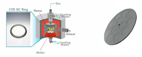
Focus Ring and SiC-Coated Graphite Susceptor
The low reactivity of CVD SiC with chlorine- and fluorine-based etching gases, coupled with its low electrical conductivity, makes it an ideal material for components like focus rings in plasma etching equipment. A focus ring, positioned around the wafer periphery, is a critical component that focuses the plasma onto the wafer surface by applying a voltage to the ring, thereby enhancing processing uniformity.
As IC miniaturization advances, the power and energy requirements of etching plasmas continue to rise, particularly in Capacitively Coupled Plasma (CCP) etching equipment. Consequently, the adoption of SiC-based focus rings is increasing rapidly due to their ability to withstand these increasingly aggressive plasma environments.**
Semicorex, as an experienced manufacturer and supplier, provides with Specialty Graphite and Ceramics Materials for Semiconductor and Photovoltaic industry. If you have any inquiries or need additional details, please don't hesitate to get in touch with us.
Contact phone # +86-13567891907
Email: sales@semicorex.com