- English
- Español
- Português
- русский
- Français
- 日本語
- Deutsch
- tiếng Việt
- Italiano
- Nederlands
- ภาษาไทย
- Polski
- 한국어
- Svenska
- magyar
- Malay
- বাংলা ভাষার
- Dansk
- Suomi
- हिन्दी
- Pilipino
- Türkçe
- Gaeilge
- العربية
- Indonesia
- Norsk
- تمل
- český
- ελληνικά
- український
- Javanese
- فارسی
- தமிழ்
- తెలుగు
- नेपाली
- Burmese
- български
- ລາວ
- Latine
- Қазақша
- Euskal
- Azərbaycan
- Slovenský jazyk
- Македонски
- Lietuvos
- Eesti Keel
- Română
- Slovenski
- मराठी
- Srpski језик

Silicon Carbide Substrate Core Process Flow
2024-07-12
Silicon carbide substrate is a compound semiconductor single crystal material composed of two elements, carbon and silicon. It has the characteristics of large bandgap, high thermal conductivity, high critical breakdown field strength, and high electron saturation drift rate. According to different downstream application fields, the core classification includes:
1) Conductive type: It can be further made into power devices such as Schottky diodes, MOSFET, IGBT, etc., which are used in new energy vehicles, rail transportation, and high-power transmission and transformation.
2) Semi-insulating type: It can be further made into microwave radio frequency devices such as HEMT, which are used in information communication, radio detection and other fields.
Conductive SiC substrates are mainly used in new energy vehicles, photovoltaics and other fields. Semi-insulating SiC substrates are mainly used in 5G radio frequency and other fields. The current mainstream 6-inch SiC substrate started abroad around 2010, and the overall gap between China and abroad in the SiC field is smaller than that of traditional silicon-based semiconductors. In addition, as SiC substrates develop towards larger sizes, the gap between China and abroad is narrowing. At present, overseas leaders have made efforts to 8 inches, and downstream customers are mainly automotive grade. Domestically, the products are mainly small-sized, and 6-inch ones are expected to have large-scale mass production capabilities in the next 2-3 years, with downstream customers mainly being industrial-grade customers.
Silicon carbide substrate preparation is a technology- and process-intensive industry, and the core process flow includes:
1. Raw material synthesis: high-purity silicon powder + carbon powder are mixed according to the formula, reacted in the reaction chamber under high temperature conditions above 2,000°C, and silicon carbide particles of specific crystal form and particle size are synthesized. After crushing, screening, cleaning and other processes, high-purity silicon carbide powder raw materials that meet the requirements of crystal growth are obtained.
2. Crystal growth: The current mainstream process in the market is PVT gas phase transmission method. Silicon carbide powder is heated in a closed, vacuum growth chamber at 2300°C to sublimate it into reaction gas. It is then transferred to the surface of the seed crystal for atomic deposition and grown into a silicon carbide single crystal.
In addition, the liquid phase method will become the mainstream process in the future. The reason is that the dislocation defects in the crystal growth process of the PVT method are difficult to control. The liquid phase method can grow silicon carbide single crystals without screw dislocations, edge dislocations and almost no stacking faults because the growth process is in a stable liquid phase. This advantage provides another important direction and future development reserve for the preparation technology of high-quality large-size silicon carbide single crystals.
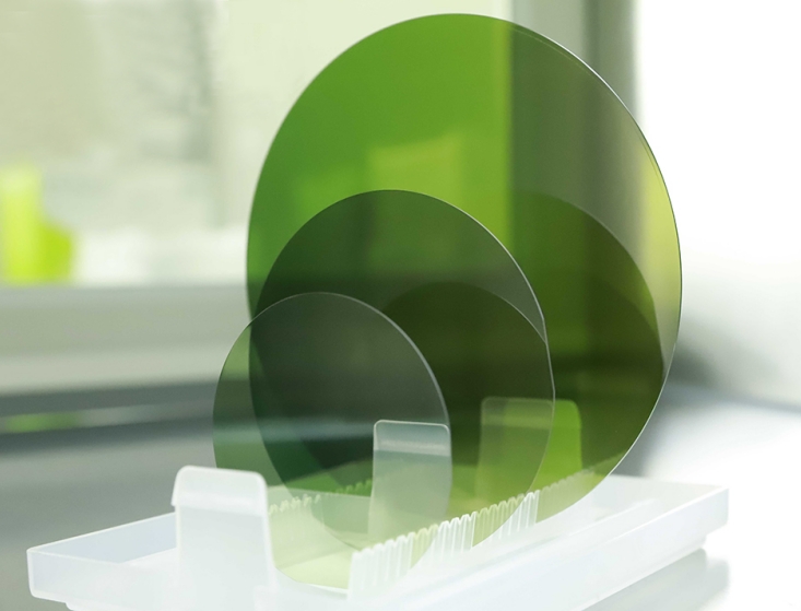
3. Crystal processing, mainly including ingot processing, crystal rod cutting, grinding, polishing, cleaning and other processes, and finally forming a silicon carbide substrate.