
- English
- Español
- Português
- русский
- Français
- 日本語
- Deutsch
- tiếng Việt
- Italiano
- Nederlands
- ภาษาไทย
- Polski
- 한국어
- Svenska
- magyar
- Malay
- বাংলা ভাষার
- Dansk
- Suomi
- हिन्दी
- Pilipino
- Türkçe
- Gaeilge
- العربية
- Indonesia
- Norsk
- تمل
- český
- ελληνικά
- український
- Javanese
- فارسی
- தமிழ்
- తెలుగు
- नेपाली
- Burmese
- български
- ລາວ
- Latine
- Қазақша
- Euskal
- Azərbaycan
- Slovenský jazyk
- Македонски
- Lietuvos
- Eesti Keel
- Română
- Slovenski
- मराठी
- Srpski језик

The Critical Role of SiC Substrates and Crystal Growth in the Semiconductor Industry
2024-07-10
Within the silicon carbide (SiC) industry chain, substrate suppliers hold significant leverage, primarily due to value distribution. SiC substrates account for 47% of the total value, followed by epitaxial layers at 23%, while device design and manufacturing constitute the remaining 30%. This inverted value chain stems from the high technological barriers inherent to substrate and epitaxial layer production.
3 major challenges plague SiC substrate growth: stringent growth conditions, slow growth rates, and demanding crystallographic requirements. These complexities contribute to increased processing difficulty, ultimately resulting in low product yields and high costs. Furthermore, the epitaxial layer’s thickness and doping concentration are critical parameters directly impacting the final device performance.
SiC Substrate Manufacturing Process:
Raw Material Synthesis: High-purity silicon and carbon powders are meticulously mixed according to a specific recipe. This mixture undergoes a high-temperature reaction (above 2000°C) to synthesize SiC particles with controlled crystal structure and particle size. Subsequent crushing, sieving, and cleaning processes yield high-purity SiC powder suitable for crystal growth.
Crystal Growth: As the most critical step in SiC substrate manufacturing, crystal growth dictates the substrate’s electrical properties. Currently, the Physical Vapor Transport (PVT) method dominates commercial SiC crystal growth. Alternatives include High-Temperature Chemical Vapor Deposition (HT-CVD) and Liquid Phase Epitaxy (LPE), though their commercial adoption remains limited.
Crystal Processing: This stage involves transforming SiC boules into polished wafers through a series of meticulous steps: ingot processing, wafer slicing, grinding, polishing, and cleaning. Each step demands high precision equipment and expertise, ultimately ensuring the quality and performance of the final SiC substrate.
1. Technical Challenges in SiC Crystal Growth:
SiC crystal growth faces several technical hurdles:
High Growth Temperatures: Exceeding 2300°C, these temperatures necessitate stringent control over both temperature and pressure within the growth furnace.
Polytypism Control: SiC exhibits over 250 polytypes, with 4H-SiC being the most desirable for electronic applications. Achieving this specific polytype demands precise control over the silicon-to-carbon ratio, temperature gradients, and gas flow dynamics during growth.
Slow Growth Rate: PVT, while commercially established, suffers from slow growth rates of approximately 0.3-0.5mm/h. Growing a 2cm crystal takes roughly 7 days, with maximum achievable crystal lengths limited to 3-5cm. This starkly contrasts with silicon crystal growth, where boules reach 2-3m in height within 72 hours, with diameters reaching 6-8 inches and even 12 inches in new facilities. This discrepancy limits SiC ingot diameters, typically ranging from 4 to 6 inches.
While Physical Vapor Transport (PVT) dominates commercial SiC crystal growth, alternative methods like High-Temperature Chemical Vapor Deposition (HT-CVD) and Liquid Phase Epitaxy (LPE) offer distinct advantages. However, overcoming their limitations and enhancing growth rates and crystal quality are crucial for broader SiC industry adoption.
Here’s a comparative overview of these crystal growth techniques:
(1) Physical Vapor Transport (PVT):
Principle: Utilizes the “sublimation-transport-recrystallization” mechanism for SiC crystal growth.
Process: High-purity carbon and silicon powders are mixed in precise ratios. The SiC powder and a seed crystal are placed at the bottom and top of a crucible within a growth furnace, respectively. Temperatures exceeding 2000°C create a temperature gradient, causing the SiC powder to sublimate and recrystallize onto the seed crystal, forming the boule.
Drawbacks: Slow growth rates (approximately 2cm in 7 days), susceptibility to parasitic reactions leading to higher defect densities in the grown crystal.
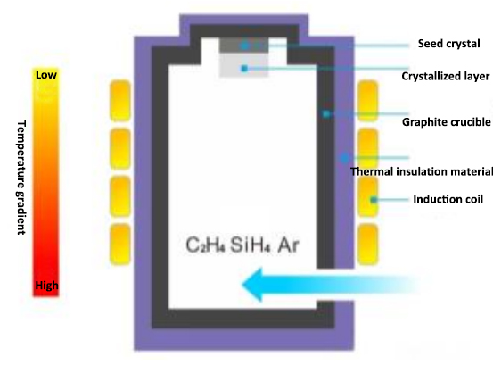
(2) High-Temperature Chemical Vapor Deposition (HT-CVD):
Principle: At temperatures between 2000-2500°C, high-purity precursor gases like silane, ethane or propane, and hydrogen are introduced into a reaction chamber. These gases decompose in the high-temperature zone, forming gaseous SiC precursors that subsequently deposit and crystallize onto a seed crystal in the lower temperature zone.
Advantages: Enables continuous crystal growth, utilizes high-purity gaseous precursors resulting in higher purity SiC crystals with fewer defects.
Drawbacks: Slow growth rates (approximately 0.4-0.5mm/h), high equipment and operational costs, susceptibility to clogging of gas inlets and outlets.
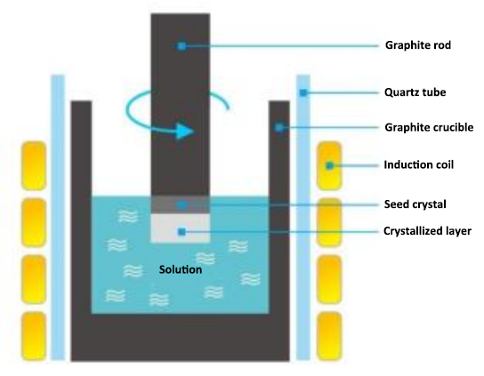
(3) Liquid Phase Epitaxy (LPE):
(While not included in your excerpt, I’m adding a brief overview of LPE for completeness.)
Principle: Employs a “dissolution-precipitation” mechanism. At temperatures ranging from 1400-1800°C, carbon is dissolved in a high-purity silicon melt. SiC crystals precipitate out of the supersaturated solution as it cools.
Advantages: Lower growth temperatures reduce thermal stresses during cooling, resulting in lower defect densities and higher crystal quality. Offers significantly faster growth rates compared to PVT.
Drawbacks: Prone to metal contamination from the crucible, limited in achievable crystal sizes, primarily confined to laboratory-scale growth.
Each method presents unique advantages and limitations. Selecting the optimal growth technique depends on specific application requirements, cost considerations, and desired crystal characteristics.
2. SiC Crystal Processing Challenges and Solutions:
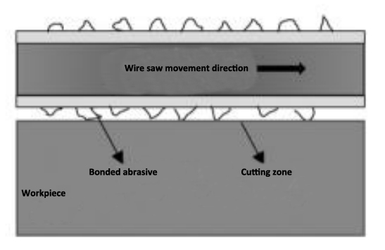
Wafer Slicing: SiC’s hardness, brittleness, and abrasion resistance make slicing challenging. Traditional diamond wire sawing is time-consuming, wasteful, and costly. Solutions include laser dicing and cold splitting techniques to improve slicing efficiency and wafer yield.
Wafer Thinning: SiC’s low fracture toughness makes it prone to cracking during thinning, hindering uniform thickness reduction. Current techniques rely on rotational grinding, which suffers from wheel wear and surface damage. Advanced methods like ultrasonic vibration-assisted grinding and electrochemical mechanical polishing are being explored to enhance material removal rates and minimize surface defects.
3. Future Outlook:
Optimizing SiC crystal growth and wafer processing is crucial for widespread SiC adoption. Future research will focus on increasing growth rates, improving crystal quality, and enhancing wafer processing efficiency to unlock the full potential of this promising semiconductor material.**


