- English
- Español
- Português
- русский
- Français
- 日本語
- Deutsch
- tiếng Việt
- Italiano
- Nederlands
- ภาษาไทย
- Polski
- 한국어
- Svenska
- magyar
- Malay
- বাংলা ভাষার
- Dansk
- Suomi
- हिन्दी
- Pilipino
- Türkçe
- Gaeilge
- العربية
- Indonesia
- Norsk
- تمل
- český
- ελληνικά
- український
- Javanese
- فارسی
- தமிழ்
- తెలుగు
- नेपाली
- Burmese
- български
- ລາວ
- Latine
- Қазақша
- Euskal
- Azərbaycan
- Slovenský jazyk
- Македонски
- Lietuvos
- Eesti Keel
- Română
- Slovenski
- मराठी
- Srpski језик
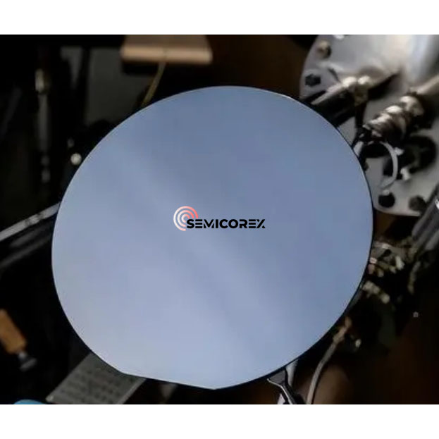
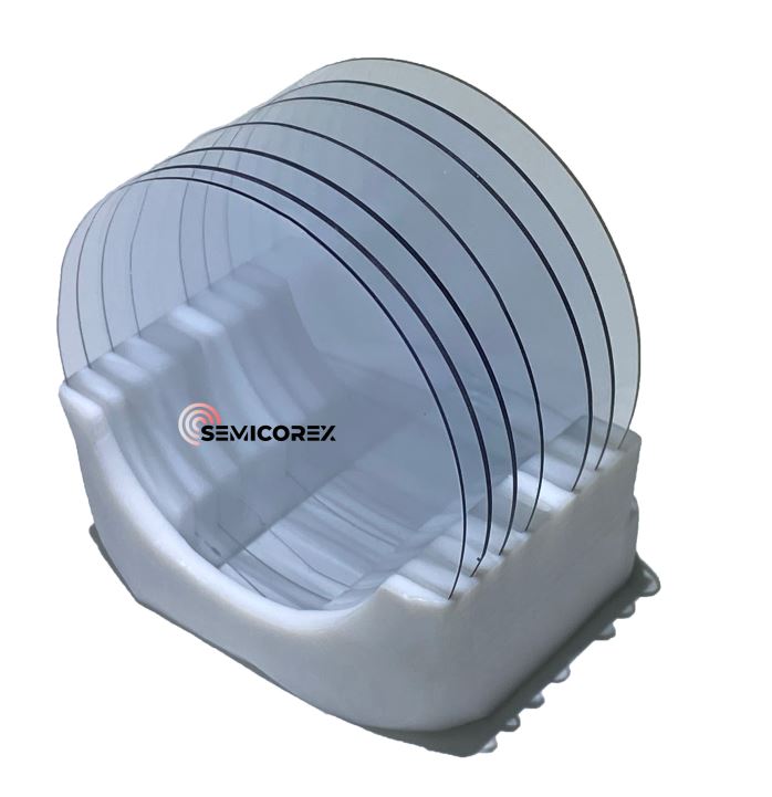
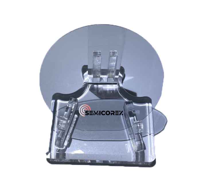
Ga2O3 Substrate
Unlock the potential of cutting-edge semiconductor applications with our Ga2O3 Substrate, a revolutionary material at the forefront of semiconductor innovation. Ga2O3, a fourth-generation wide-bandgap semiconductor, exhibits unparalleled characteristics that redefine power device performance and reliability.
Send Inquiry
Ga2O3 stands out as a wide-bandgap semiconductor, ensuring stability and resilience in extreme conditions, making it ideal for high-temperature and high-radiation environments.
With a high breakdown field strength and exceptional Baliga values, Ga2O3 excels in high-voltage and high-power applications, offering unmatched reliability and low power losses.
Ga2O3 outshines traditional materials with its superior power performance. The Baliga values for Ga2O3 are four times that of GaN and ten times that of SiC, translating to excellent conduction characteristics and power efficiency. Ga2O3 devices exhibit power losses only 1/7th of SiC and an impressive 1/49th of silicon-based devices.
Ga2O3's lower hardness compared to SiC simplifies the manufacturing process, resulting in lower processing costs. This advantage positions Ga2O3 as a cost-effective alternative for various applications.
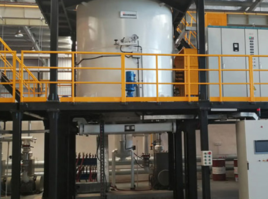
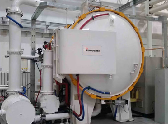
Grown using a liquid-phase melt method, Ga2O3 boasts superior crystal quality with a remarkably low defect density, outperforming SiC, which is grown using a vapor-phase method.
Ga2O3 exhibits a growth rate 100 times faster than SiC, contributing to higher production efficiency and, consequently, reduced manufacturing costs.
Applications:
Power Devices: Ga2O3 substrate is poised to revolutionize power devices, offering four major opportunities:
Unipolar devices replacing bipolar devices: MOSFETs replacing IGBTs in applications such as new energy vehicles, charging stations, high-voltage power supplies, industrial power control, and more.
Enhanced Energy Efficiency: Ga2O3 substrate power devices are energy-efficient, aligning with strategies for carbon neutrality and peak carbon emissions reduction.
Large-Scale Production: With simplified processing and cost-effective chip fabrication, Ga2O3 substrate facilitates large-scale production.
High Reliability: Ga2O3 substrate with stable material properties and reliable structure make it suitable for high-reliability applications, ensuring longevity and consistent performance.
RF Devices: Ga2O3 substrate is a game-changer in the RF (Radio Frequency) device market. Its advantages include:
Crystal Quality: The Ga2O3substrate allows for high-quality epitaxial growth, overcoming lattice mismatch issues associated with other substrates.
Cost-Effective Growth: Ga2O3's cost-effective growth on large substrates, particularly on 6-inch wafers, makes it a competitive option for RF applications.
Potential in GaN RF Devices: The minimal lattice mismatch with GaN positions Ga2O3 as an ideal substrate for high-performance GaN RF devices.
Embrace the future of semiconductor technology with Ga2O3 Substrate, where groundbreaking properties meet limitless possibilities. Revolutionize your power and RF applications with a material designed for excellence and efficiency.

