- English
- Español
- Português
- русский
- Français
- 日本語
- Deutsch
- tiếng Việt
- Italiano
- Nederlands
- ภาษาไทย
- Polski
- 한국어
- Svenska
- magyar
- Malay
- বাংলা ভাষার
- Dansk
- Suomi
- हिन्दी
- Pilipino
- Türkçe
- Gaeilge
- العربية
- Indonesia
- Norsk
- تمل
- český
- ελληνικά
- український
- Javanese
- فارسی
- தமிழ்
- తెలుగు
- नेपाली
- Burmese
- български
- ລາວ
- Latine
- Қазақша
- Euskal
- Azərbaycan
- Slovenský jazyk
- Македонски
- Lietuvos
- Eesti Keel
- Română
- Slovenski
- मराठी
- Srpski језик
SOI Wafers
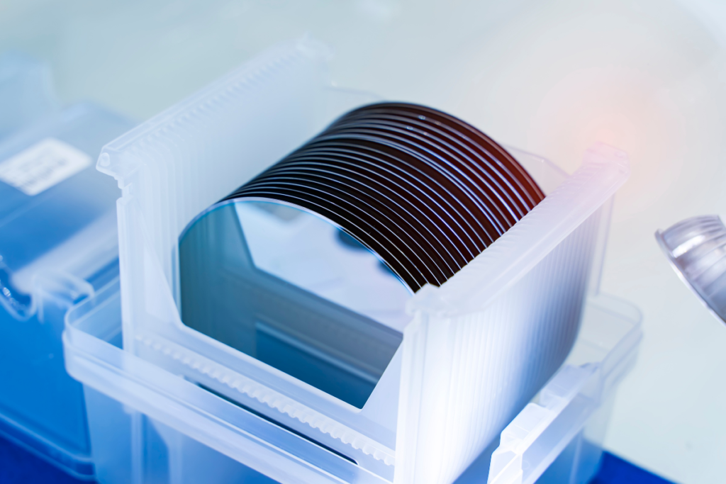
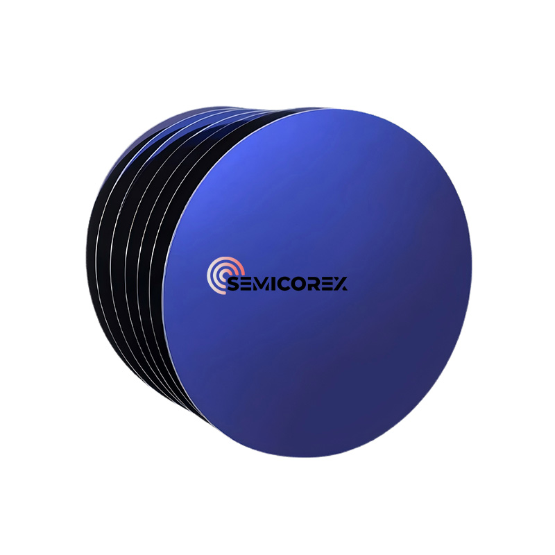
Semicorex SOI Wafers represent a critical advancement in this field, offering numerous advantages over traditional silicon wafers. At Semicorex, we are proud to manufacture and supply SOI wafers that meet the rigorous demands of modern semiconductor applications.*
Send Inquiry
Semicorex SOI Wafers are a specialized type of substrate used in the fabrication of semiconductor devices. Unlike conventional silicon wafers, SOI wafers have an additional insulating layer, typically made of silicon dioxide (SiO2), which separates a thin layer of silicon from the bulk silicon substrate. This unique structure allows for significant improvements in device performance, power efficiency, and reliability, making SOI wafers an essential component in the production of advanced microelectronics, telecommunications, and high-performance computing systems.
Composition and Structure
SOI wafers consist of three main layers:
Top Silicon Layer: The top layer is a thin, high-quality silicon layer where the active devices, such as transistors, are fabricated. The thickness of this layer can vary depending on the specific application but typically ranges from a few nanometers to several micrometers.
Buried Oxide Layer (BOX): This is the insulating layer made of silicon dioxide (SiO2), which electrically isolates the top silicon layer from the bulk substrate. The thickness of the BOX layer can also vary but is usually between 100 nm and 2 µm. This insulation plays a critical role in reducing parasitic capacitance, improving the overall performance of the device.
Silicon Substrate: The bottom layer is the bulk silicon, which provides mechanical support to the wafer. The substrate can be standard silicon or a more specialized material depending on the specific requirements of the end product.
The thickness and composition of each layer can be customized to meet the precise needs of various applications, making SOI wafers highly versatile and adaptable to a wide range of semiconductor technologies.

Applications of SOI Wafers
SOI wafers are used across a wide range of industries and applications, particularly in areas where high performance, low power consumption, and reliability are paramount. Some key applications include:
Microprocessors and High-Performance Computing (HPC): SOI wafers are commonly used in the fabrication of high-speed microprocessors and HPC systems, where the reduced parasitic capacitance and improved thermal management contribute to faster processing speeds and lower power consumption.
Telecommunications: The ability to operate at high frequencies with minimal signal loss makes SOI wafers ideal for RF (radio frequency) and mixed-signal applications, which are critical in telecommunications equipment, including 5G infrastructure.
Automotive Electronics: In the automotive industry, SOI wafers are used to produce sensors, microcontrollers, and other electronic components that require high reliability and resistance to harsh operating conditions, such as extreme temperatures and radiation.
Consumer Electronics: The demand for portable, battery-operated devices such as smartphones, tablets, and wearables has driven the adoption of SOI technology due to its power efficiency and ability to deliver high performance in a compact form factor.
Aerospace and Defense: The radiation hardness and reliability of SOI wafers make them ideal for use in aerospace and defense applications, where devices must withstand extreme environmental conditions, including high levels of radiation and temperature fluctuations.
Semicorex SOI wafers represent a significant advancement in semiconductor technology, offering numerous advantages over traditional silicon wafers. Their ability to reduce power consumption, improve device performance, and enable more aggressive scaling makes them a critical component in the development of next-generation electronic devices. At Semicorex, we are dedicated to providing high-quality SOI wafers that meet the stringent requirements of our customers across various industries. With our commitment to innovation and quality, we continue to push the boundaries of semiconductor technology, enabling the creation of faster, smaller, and more efficient electronic devices for the future.


