
- English
- Español
- Português
- русский
- Français
- 日本語
- Deutsch
- tiếng Việt
- Italiano
- Nederlands
- ภาษาไทย
- Polski
- 한국어
- Svenska
- magyar
- Malay
- বাংলা ভাষার
- Dansk
- Suomi
- हिन्दी
- Pilipino
- Türkçe
- Gaeilge
- العربية
- Indonesia
- Norsk
- تمل
- český
- ελληνικά
- український
- Javanese
- فارسی
- தமிழ்
- తెలుగు
- नेपाली
- Burmese
- български
- ລາວ
- Latine
- Қазақша
- Euskal
- Azərbaycan
- Slovenský jazyk
- Македонски
- Lietuvos
- Eesti Keel
- Română
- Slovenski
- मराठी
- Srpski језик
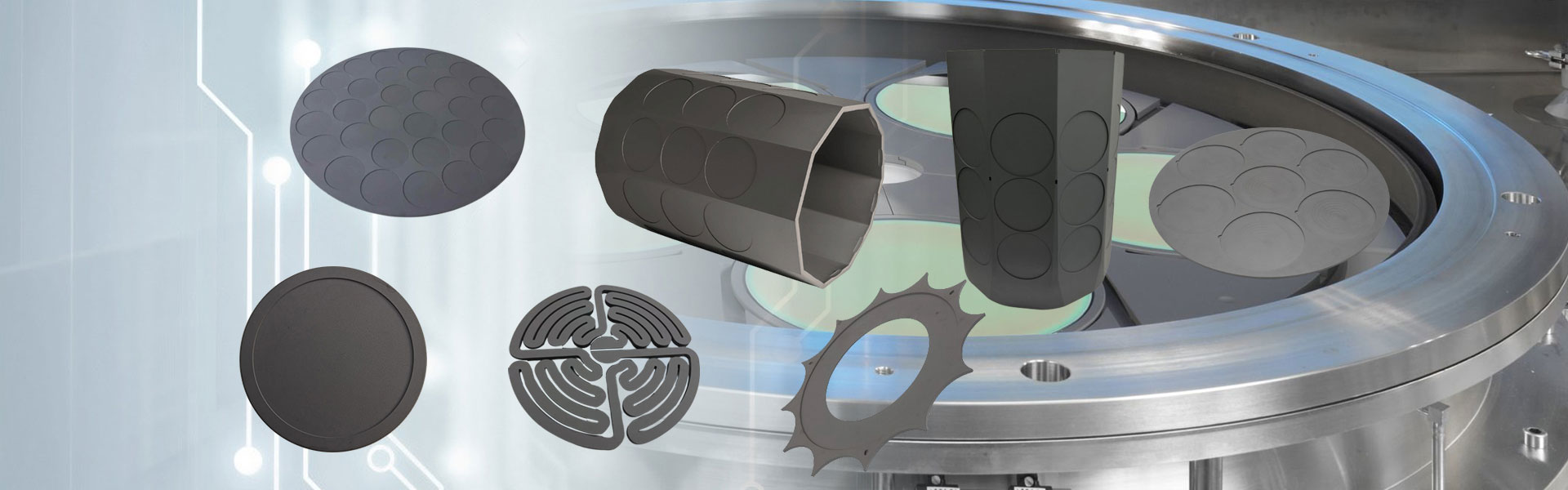


Silicon on Insulator Wafers
Semicorex Silicon on Insulator Wafers are advanced semiconductor materials that enable superior performance, reduced power consumption, and enhanced device scalability. Choosing Semicorex's SOI wafers ensures you receive top-tier, precision-engineered products, backed by our expertise and commitment to innovation, reliability, and quality.*
Send Inquiry
Product Description
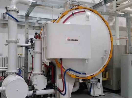
Semicorex Silicon-on-Insulator wafers are a key material in the development of advanced semiconductor devices, providing a range of advantages that are unattainable with standard bulk silicon wafers. Silicon on Insulator Wafers consist of a layered structure in which a thin, high-quality silicon layer is separated from the underlying bulk silicon by an insulating layer, typically made of silicon dioxide (SiO₂). This configuration enables significant improvements in speed, power efficiency, and thermal performance, making Silicon on Insulator Wafers an essential material for high-performance and low-power applications in industries such as consumer electronics, automotive, telecommunications, and aerospace.
SOI Wafer Structure and Fabrication
The structure of an Silicon on Insulator Wafers is carefully engineered to enhance device performance while addressing the limitations of traditional silicon wafers. Silicon on Insulator Wafers are typically fabricated using one of two main techniques: Separation by Implantation of Oxygen (SIMOX) or Smart Cut™ technology.
● Top Silicon Layer: This layer, often referred to as the active layer, is a thin, high-purity silicon layer where electronic devices are built. The thickness of this layer can be precisely controlled to meet the requirements of specific applications, typically ranging from a few nanometers to several microns.
● Buried ●Oxide Layer (BOX): The BOX layer is the key to the performance of SOI wafers. This silicon dioxide layer serves as an insulator, isolating the active silicon layer from the bulk substrate. It helps reduce unwanted electrical interactions, such as parasitic capacitance, and contributes to lower power consumption and higher switching speeds in the final device.
● Silicon Substrate: Below the BOX layer is the bulk silicon substrate, which provides the mechanical stability needed for wafer handling and processing. Though the substrate itself does not directly participate in the electronic performance of the device, its role in supporting the upper layers is critical to the structural integrity of the wafer.
By utilizing advanced fabrication techniques, the precise thickness and uniformity of each layer can be tailored to the specific needs of various semiconductor applications, making SOI wafers highly adaptable.
Key Benefits of Silicon-on-Insulator Wafers
The unique structure of Silicon on Insulator Wafers delivers several advantages over traditional bulk silicon wafers, particularly in terms of performance, power efficiency, and scalability:
Enhanced Performance: Silicon on Insulator Wafers reduce parasitic capacitance between transistors, which in turn leads to faster signal transmission and higher overall device speeds. This performance boost is especially important for applications requiring high-speed processing, such as microprocessors, high-performance computing (HPC), and networking equipment.
Lower Power Consumption: Silicon on Insulator Wafers enable devices to operate at lower voltages while maintaining high performance. The insulation provided by the BOX layer reduces leakage currents, allowing for more efficient power usage. This makes SOI wafers ideal for battery-powered devices, where power efficiency is critical to extending battery life.
Improved Thermal Management: The insulating properties of the BOX layer contribute to better heat dissipation and thermal isolation. This helps prevent hotspots and improves the thermal performance of the device, allowing for more reliable operation in high-power or high-temperature environments.
Greater Scalability: As transistor sizes shrink and device densities increase, Silicon on Insulator Wafers offer a more scalable solution compared to bulk silicon. The reduced parasitic effects and improved isolation allow for smaller, faster transistors, making SOI wafers well-suited for advanced semiconductor nodes.
Reduced Short-Channel Effects: SOI technology helps mitigate short-channel effects, which can degrade the performance of transistors in deeply scaled semiconductor devices. The isolation provided by the BOX layer reduces the electrical interference between neighboring transistors, enabling better performance at smaller geometries.
Radiation Resistance: The inherent radiation resistance of Silicon on Insulator Wafers makes them ideal for use in environments where exposure to radiation is a concern, such as in aerospace, defense, and nuclear applications. The BOX layer helps protect the active silicon layer from radiation-induced damage, ensuring reliable operation in harsh conditions.
Semicorex Silicon-on-Insulator wafers are a groundbreaking material in the semiconductor industry, offering unparalleled performance, power efficiency, and scalability. As the demand for faster, smaller, and more energy-efficient devices continues to grow, SOI technology is poised to play an increasingly important role in the future of electronics. At Semicorex, we are dedicated to providing our customers with high-quality SOI wafers that meet the rigorous demands of today’s most advanced applications. Our commitment to excellence ensures that our Silicon on Insulator Wafers deliver the reliability and performance required for the next generation of semiconductor devices.
Hot Tags: Silicon on Insulator Wafers, China, Manufacturers, Suppliers, Factory, Customized, Bulk, Advanced, Durable
Product Tag
Related Category
Send Inquiry
Please feel free to give your inquiry in the form below. We will reply you in 24 hours.


