- English
- Español
- Português
- русский
- Français
- 日本語
- Deutsch
- tiếng Việt
- Italiano
- Nederlands
- ภาษาไทย
- Polski
- 한국어
- Svenska
- magyar
- Malay
- বাংলা ভাষার
- Dansk
- Suomi
- हिन्दी
- Pilipino
- Türkçe
- Gaeilge
- العربية
- Indonesia
- Norsk
- تمل
- český
- ελληνικά
- український
- Javanese
- فارسی
- தமிழ்
- తెలుగు
- नेपाली
- Burmese
- български
- ລາວ
- Latine
- Қазақша
- Euskal
- Azərbaycan
- Slovenský jazyk
- Македонски
- Lietuvos
- Eesti Keel
- Română
- Slovenski
- मराठी
- Srpski језик
What is Semiconductor Ion Implantation Technology?
2025-01-02
How Does Ion Implantation Work?
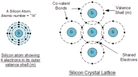
In semiconductor manufacturing, ion implantation involves using high-energy accelerators to inject specific impurity atoms, such as arsenic or boron, into a silicon substrate. Silicon, positioned at the 14th place in the periodic table, forms covalent bonds by sharing its four outer electrons with neighboring atoms. This process alters the electrical properties of the silicon, adjusting transistor threshold voltages and forming source and drain structures.

A physicist once pondered the effects of introducing different atoms into the silicon lattice. By adding arsenic, which has five outer electrons, one electron remains free, enhancing the silicon’s conductivity and transforming it into an n-type semiconductor. Conversely, introducing boron, with only three outer electrons, creates a positive hole, resulting in a p-type semiconductor. This method of incorporating different elements into the silicon lattice is known as ion implantation.
What Are the Components of Ion Implantation Equipment?
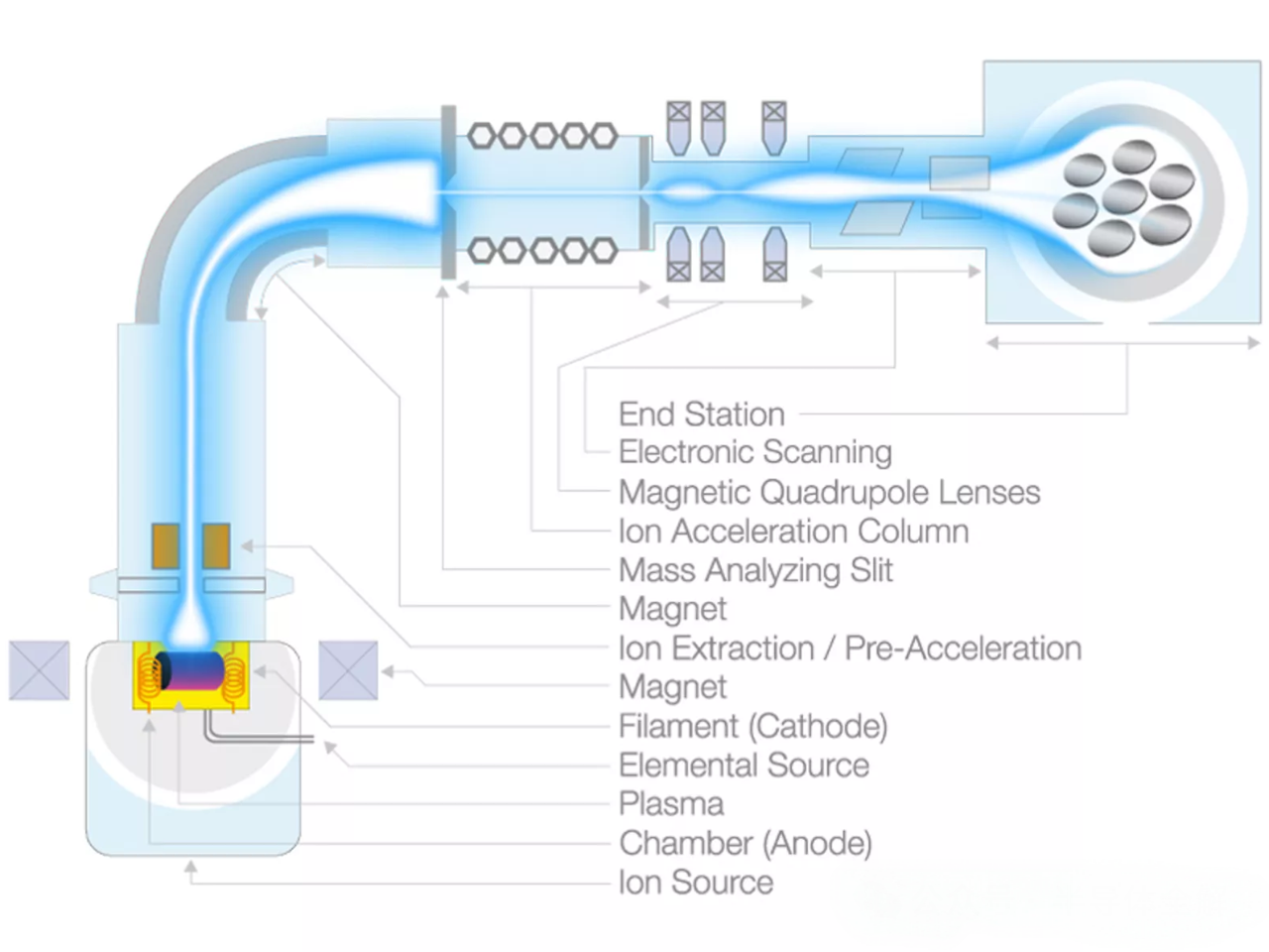
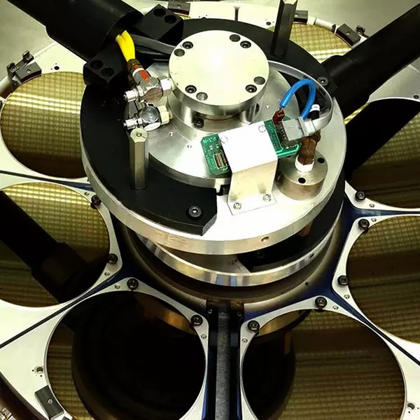
Ion implantation equipment consists of several key components: an ion source, an electric acceleration system, a vacuum system, an analysis magnet, a beam path, a post-acceleration system, and an implantation chamber. The ion source is crucial, as it strips electrons from atoms to form positive ions, which are then extracted to form an ion beam.

This beam passes through a mass analysis module, selectively isolating the desired ions for semiconductor modification. After mass analysis, the high-purity ion beam is focused and shaped, accelerated to the required energy, and scanned uniformly across the semiconductor substrate. High-energy ions penetrate the material, embedding into the lattice, which can create defects beneficial for certain applications, such as isolating regions on chips and integrated circuits. For other applications, annealing cycles are used to repair damage and activate dopants, enhancing material conductivity.

What Are the Principles of Ion Implantation?
Ion implantation is a technique for introducing dopants into semiconductors, playing a vital role in integrated circuit fabrication. The process involves:
Ion Purification: Ions generated from the source, carrying different electron and proton numbers, are accelerated to form a positive/negative ion beam. Impurities are filtered based on charge-to-mass ratio to achieve the desired ion purity.
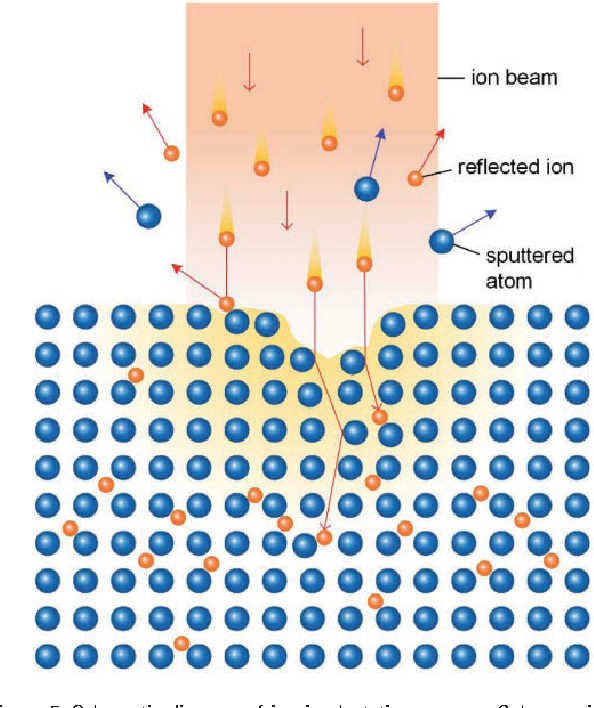
Ion Injection: The accelerated ion beam is directed at a specific angle to the target crystal surface, uniformly irradiating the wafer. After penetrating the surface, ions undergo collisions and scattering within the lattice, eventually settling at a certain depth, modifying the material’s properties. Patterned doping can be achieved using physical or chemical masks, allowing precise electrical modifications of specific circuit areas.
The expected depth distribution of dopants is determined by the beam’s energy, angle, and the wafer’s material properties.
What Are the Advantages and Limitations of Ion Implantation?
Advantages:
Wide Range of Dopants: Almost all elements from the periodic table can be used, with high purity ensured by precise ion selection.
Precise Control: The energy and angle of the ion beam can be accurately controlled, allowing precise depth and concentration distribution of dopants.
Flexibility: Ion implantation is not limited by the wafer’s solubility limits, allowing higher concentrations than other methods.
Uniform Doping: Large-area uniform doping is achievable.
Temperature Control: The wafer’s temperature can be controlled during implantation.

Limitations:
Shallow Depth: Typically limited to about one micron from the surface.
Difficulties with Very Shallow Implantation: Low-energy beams are hard to control, increasing process time and cost.
Lattice Damage: Ions can damage the lattice, requiring post-implantation annealing to repair and activate dopants.
High Cost: Equipment and process costs are significant.
We at Semicorex specialize in Graphite/Ceramics with proprietary CVD Coating solutions in ion implantion, if you have any inquiries or need additional details, please don't hesitate to get in touch with us.
Contact phone: +86-13567891907
Email: sales@semicorex.com


