
- English
- Español
- Português
- русский
- Français
- 日本語
- Deutsch
- tiếng Việt
- Italiano
- Nederlands
- ภาษาไทย
- Polski
- 한국어
- Svenska
- magyar
- Malay
- বাংলা ভাষার
- Dansk
- Suomi
- हिन्दी
- Pilipino
- Türkçe
- Gaeilge
- العربية
- Indonesia
- Norsk
- تمل
- český
- ελληνικά
- український
- Javanese
- فارسی
- தமிழ்
- తెలుగు
- नेपाली
- Burmese
- български
- ລາວ
- Latine
- Қазақша
- Euskal
- Azərbaycan
- Slovenský jazyk
- Македонски
- Lietuvos
- Eesti Keel
- Română
- Slovenski
- मराठी
- Srpski језик
SiGe and Si Selective Etching Technology
2024-12-20
The Gate-All-Around FET (GAAFET), as a next-generation transistor architecture poised to replace the FinFET, has garnered significant attention for its ability to provide superior electrostatic control and enhanced performance at smaller dimensions. A critical step in the fabrication of n-type GAAFETs involves the high-selectivity etching of SiGe:Si stacks prior to the deposition of inner spacers, generating silicon nanosheets and releasing channels.
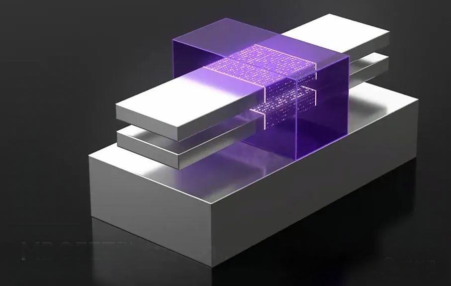
This article delves into the selective etching technologies involved in this process and introduces two novel etching methods—high oxidative gas plasma-free etching and atomic layer etching (ALE)—which offer new solutions for achieving high precision and selectivity in SiGe etching.
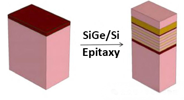
SiGe Superlattice Layers in GAA Structures
In the design of GAAFETs, to enhance device performance, alternating layers of Si and SiGe are epitaxially grown on a silicon substrate, forming a multilayer structure known as a superlattice. These SiGe layers not only adjust the carrier concentration but also improve electron mobility by introducing stress. However, in subsequent process steps, these SiGe layers need to be precisely removed while retaining the silicon layers, requiring highly selective etching technologies.
Methods for Selective Etching of SiGe
High Oxidative Gas Plasma-Free Etching
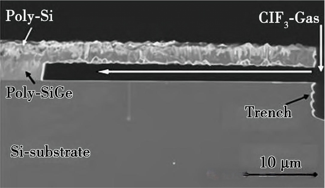
The selection of ClF3 gas: This etching method employs highly oxidative gases with extreme selectivity, such as ClF3, achieving a SiGe:Si selectivity ratio of 1000-5000. It can be completed at room temperature without causing plasma damage.
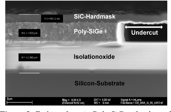
Low-temperature efficiency: The optimal temperature is around 30°C, realizing high-selectivity etching under low-temperature conditions, avoiding additional thermal budget increases, which is crucial for maintaining device performance.
Dry environment: The entire etching process is conducted under completely dry conditions, eliminating the risk of structure adhesion.
Atomic Layer Etching (ALE)
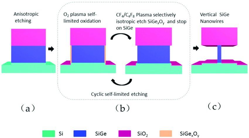
Self-limiting characteristics: ALE is a two-step cyclic etching technology, where the surface of the material to be etched is first modified, and then the modified layer is removed without affecting the unmodified parts. Each step is self-limiting, ensuring precision to the level of removing just a few atomic layers at a time.
Cyclic etching: The aforementioned two steps are repeatedly cycled until the desired etching depth is achieved. This process enables ALE to achieve atomic-level precision etching in small-sized cavities on the inner walls.
We at Semicorex specialize in SiC/TaC coated graphite solutions applied in Etching Processes in semiconductor manufacturing, if you have any inquiries or need additional details, please don't hesitate to get in touch with us.
Contact phone: +86-13567891907
Email: sales@semicorex.com


