- English
- Español
- Português
- русский
- Français
- 日本語
- Deutsch
- tiếng Việt
- Italiano
- Nederlands
- ภาษาไทย
- Polski
- 한국어
- Svenska
- magyar
- Malay
- বাংলা ভাষার
- Dansk
- Suomi
- हिन्दी
- Pilipino
- Türkçe
- Gaeilge
- العربية
- Indonesia
- Norsk
- تمل
- český
- ελληνικά
- український
- Javanese
- فارسی
- தமிழ்
- తెలుగు
- नेपाली
- Burmese
- български
- ລາວ
- Latine
- Қазақша
- Euskal
- Azərbaycan
- Slovenský jazyk
- Македонски
- Lietuvos
- Eesti Keel
- Română
- Slovenski
- मराठी
- Srpski језик
SiGe in Chip Manufacturing: A Professional News Report
The Evolution of Semiconductor Materials
In the realm of modern semiconductor technology, the relentless drive towards miniaturization has pushed the limits of traditional silicon-based materials. To meet the demands for high performance and low power consumption, SiGe (Silicon Germanium) has emerged as a composite material of choice in semiconductor chip manufacturing due to its unique physical and electrical properties. This article delves into the epitaxy process of SiGe and its role in epitaxial growth, strained silicon applications, and Gate-All-Around (GAA) structures.

The Significance of SiGe Epitaxy
1.1 Introduction to Epitaxy in Chip Manufacturing:
Epitaxy, often abbreviated as Epi, refers to the growth of a single-crystal layer on a single-crystal substrate with the same lattice arrangement. This layer can be either homoepitaxial (such as Si/Si) or heteroepitaxial (such as SiGe/Si or SiC/Si). Various methods are employed for epitaxial growth, including Molecular Beam Epitaxy (MBE), Ultra-High Vacuum Chemical Vapor Deposition (UHV/CVD), Atmospheric and Reduced Pressure Epitaxy (ATM & RP Epi). This article focuses on the epitaxy processes of silicon (Si) and silicon-germanium (SiGe) widely used in semiconductor integrated circuit production with silicon as the substrate material.
1.2 Advantages of SiGe Epitaxy:
Incorporating a certain proportion of germanium (Ge) during the epitaxy process forms a SiGe single-crystal layer that not only reduces the bandgap width but also increases the transistor's cut-off frequency (fT). This makes it extensively applicable in high-frequency devices for wireless and optical communications. Moreover, in advanced CMOS integrated circuit processes, the lattice mismatch (about 4%) between Ge and Si introduces lattice stress, enhancing the mobility of electrons or holes and thus increasing the device's saturation current and response speed.

The Comprehensive SiGe Epitaxy Process Flow
2.1 Pre-treatment:
Silicon wafers are pre-treated based on the desired process outcomes, primarily involving the removal of the natural oxide layer and impurities on the wafer surface. For heavily doped substrate wafers, it is crucial to consider whether backsealing is necessary to reduce auto-doping during subsequent epitaxy growth.
2.2 Growth Gases and Conditions:
Silicon gases: Silane (SiH₄), Dichlorosilane (DCS, SiH₂Cl₂), and Trichlorosilane (TCS, SiHCl₃) are the three most commonly used silicon gas sources. SiH₄ is suitable for low-temperature full epitaxy processes, while TCS, known for its rapid growth rate, is widely used for the preparation of thick silicon epitaxy layers.
Germanium gas: Germane (GeH₄) is the primary source for adding germanium, used in conjunction with silicon sources to form SiGe alloys.
Selective epitaxy: Selective growth is achieved by adjusting the relative rates of epitaxial deposition and in situ etching, using chlorine-containing silicon gas DCS. The selectivity is due to the adsorption of Cl atoms on the silicon surface being less than that on oxides or nitrides, facilitating epitaxial growth. SiH₄, lacking Cl atoms and with low activation energy, is generally applied only to low-temperature full epitaxy processes. Another commonly used silicon source, TCS, has low vapor pressure and is liquid at room temperature, requiring H₂ bubbling to introduce it into the reaction chamber. However, it is relatively inexpensive and often used for its rapid growth rate (up to 5 μm/min) to grow thicker silicon epitaxy layers, widely applied in silicon epitaxy wafer production.

Strained Silicon in Epitaxial Layers
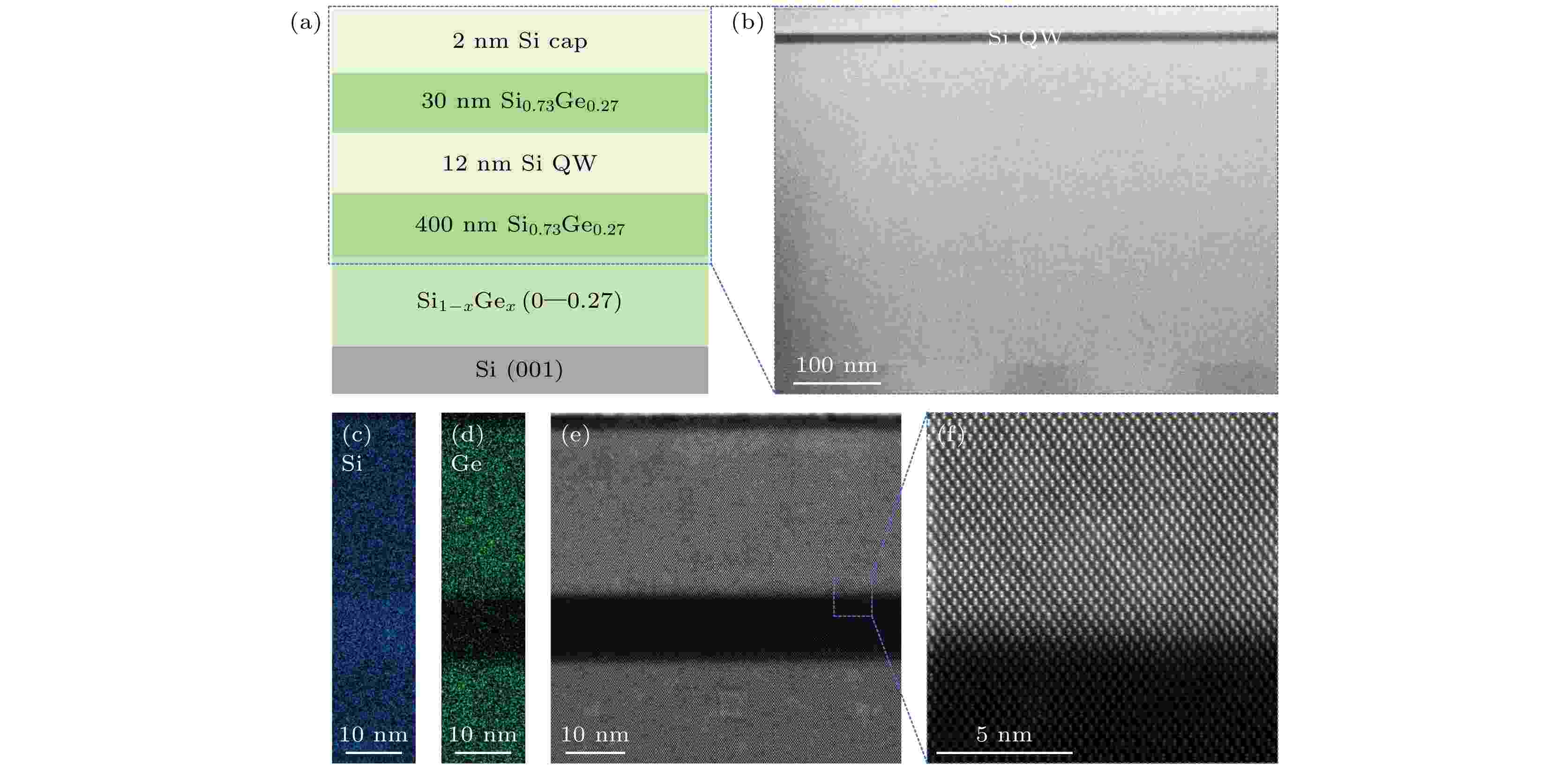
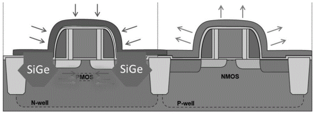
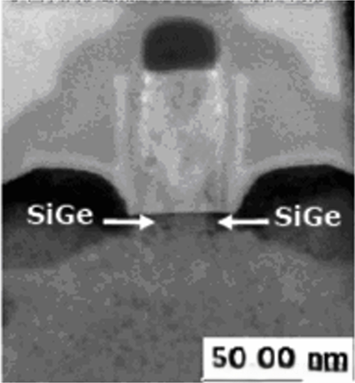
During epitaxial growth, epitaxial single-crystal Si is deposited on a relaxed SiGe layer. Due to the lattice mismatch between Si and SiGe, the Si single-crystal layer is subjected to tensile stress from the underlying SiGe layer, significantly enhancing the electron mobility in NMOS transistors. This technology not only increases saturation current (Idsat) but also improves device response speed. For PMOS devices, SiGe layers are epitaxially grown in the source and drain regions after etching to introduce compressive stress on the channel, enhancing hole mobility and increasing saturation current.

SiGe as a Sacrificial Layer in GAA Structures
In the manufacturing of Gate-All-Around (GAA) nanowire transistors, SiGe layers act as sacrificial layers. High-selectivity anisotropic etching techniques, such as quasi-atomic layer etching (quasi-ALE), allow for the precise removal of SiGe layers to form nanowire or nanosheet structures.

We at Semicorex specialize in SiC/TaC coated graphite solutions applied in Si epitaxial growth in semiconductor manufacturing, if you have any inquiries or need additional details, please don't hesitate to get in touch with us.
Contact phone: +86-13567891907
Email: sales@semicorex.com


