- English
- Español
- Português
- русский
- Français
- 日本語
- Deutsch
- tiếng Việt
- Italiano
- Nederlands
- ภาษาไทย
- Polski
- 한국어
- Svenska
- magyar
- Malay
- বাংলা ভাষার
- Dansk
- Suomi
- हिन्दी
- Pilipino
- Türkçe
- Gaeilge
- العربية
- Indonesia
- Norsk
- تمل
- český
- ελληνικά
- український
- Javanese
- فارسی
- தமிழ்
- తెలుగు
- नेपाली
- Burmese
- български
- ລາວ
- Latine
- Қазақша
- Euskal
- Azərbaycan
- Slovenský jazyk
- Македонски
- Lietuvos
- Eesti Keel
- Română
- Slovenski
- मराठी
- Srpski језик

Infineon Unveils World’s First 300mm Power GaN Wafer
2024-09-14
Recently, Infineon Technologies announced the successful development of the world’s first 300mm power Gallium Nitride (GaN) wafer technology. This makes them the first company to master this groundbreaking technology and achieve mass production within existing large-scale, high-capacity manufacturing environments. This innovation marks a significant advancement in the GaN-based power semiconductor market.
How Does the 300mm Technology Compare to the 200mm Technology?
Compared to 200mm technology, employing 300mm wafers allows for the production of 2.3 times more GaN chips per wafer, significantly enhancing production efficiency and output. This breakthrough not only consolidates Infineon’s leadership in the power systems field but also accelerates the rapid development of GaN technology.
What Did Infineon’s CEO Say About This Achievement?
Infineon Technologies CEO Jochen Hanebeck stated, “This remarkable achievement demonstrates our robust strength in innovation and is a testament to the relentless efforts of our global team. We firmly believe that this technological breakthrough will reshape industry norms and unlock the full potential of GaN technology. Nearly a year after our acquisition of GaN Systems, we are once again showcasing our determination to lead in the rapidly growing GaN market. As a leader in power systems, Infineon has gained a competitive edge in three key materials: silicon, silicon carbide, and GaN.”
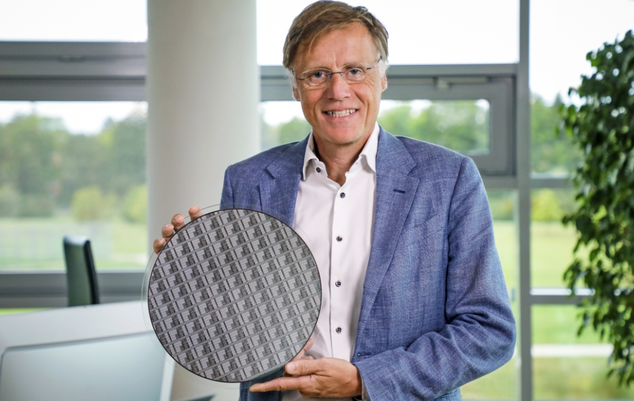
Infineon CEO Jochen Hanebeck holds one of the world’s first 300mm GaN Power wafers produced in an existing and scalable high-volume manufacturing environment
Why Is the 300mm GaN Technology Advantageous?
One significant advantage of the 300mm GaN technology is that it can be produced using existing 300mm silicon manufacturing equipment, as GaN and silicon share similarities in manufacturing processes. This feature allows Infineon to seamlessly integrate GaN technology into its current production systems, thereby accelerating the technology’s adoption and application.
Where Has Infineon Successfully Produced 300mm GaN Wafers?
Currently, Infineon has successfully manufactured 300mm GaN wafers on the existing 300mm silicon production lines at its power plant in Villach, Austria. Building on the established foundation of 200mm GaN technology and 300mm silicon production, the company has further expanded its technological and production capabilities.
What Does This Breakthrough Mean for the Future?
This breakthrough not only highlights Infineon’s strengths in innovation and large-scale production capabilities but also lays a solid foundation for the future development of the power semiconductor industry. As GaN technology continues to evolve, Infineon will persist in driving market growth, further enhancing its leadership position in the global semiconductor industry.**