- English
- Español
- Português
- русский
- Français
- 日本語
- Deutsch
- tiếng Việt
- Italiano
- Nederlands
- ภาษาไทย
- Polski
- 한국어
- Svenska
- magyar
- Malay
- বাংলা ভাষার
- Dansk
- Suomi
- हिन्दी
- Pilipino
- Türkçe
- Gaeilge
- العربية
- Indonesia
- Norsk
- تمل
- český
- ελληνικά
- український
- Javanese
- فارسی
- தமிழ்
- తెలుగు
- नेपाली
- Burmese
- български
- ລາວ
- Latine
- Қазақша
- Euskal
- Azərbaycan
- Slovenský jazyk
- Македонски
- Lietuvos
- Eesti Keel
- Română
- Slovenski
- मराठी
- Srpski језик

Monocrystalline Silicon Manufacturing
2024-09-13
Monocrystalline silicon is a fundamental material used in the production of large-scale integrated circuits, chips, and solar cells. As the traditional base for semiconductor devices, silicon-based chips remain a cornerstone of modern electronics. The growth of monocrystalline silicon, particularly from a molten state, is crucial to ensuring high-quality, defect-free crystals that meet the stringent demands of industries such as electronics and photovoltaics. Several techniques are employed to grow single crystals from a molten state, each with its own advantages and specific applications. The three primary methods used in monocrystalline silicon manufacturing are the Czochralski (CZ) method, the Kyropoulos method, and the Float Zone (FZ) method.
1. Czochralski Method (CZ)
The Czochralski method is one of the most widely used processes for growing monocrystalline silicon from a molten state. This method involves rotating and pulling a seed crystal from a silicon melt under controlled temperature conditions. As the seed crystal is gradually lifted, it pulls silicon atoms from the melt, which arrange themselves into a single crystalline structure that matches the orientation of the seed crystal.
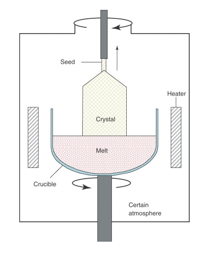
Advantages of the Czochralski Method:
High-Quality Crystals: The Czochralski method allows for the rapid growth of high-quality crystals. The process can be continuously monitored, allowing for real-time adjustments to ensure optimal crystal growth.
Low Stress and Minimal Defects: During the growth process, the crystal does not come into direct contact with the crucible, reducing internal stress and avoiding unwanted nucleation on the crucible walls.
Adjustable Defect Density: By fine-tuning the growth parameters, the dislocation density in the crystal can be minimized, resulting in highly complete and uniform crystals.
The basic form of the Czochralski method has been modified over time to address certain limitations, particularly regarding crystal size. Traditional CZ methods are generally restricted to producing crystals with diameters of around 51 to 76 mm. To overcome this limitation and grow larger crystals, several advanced techniques have been developed, such as the Liquid Encapsulated Czochralski (LEC) method and the Guided Mold method.
Liquid Encapsulated Czochralski (LEC) Method: This modified technique was developed to grow volatile III-V compound semiconductor crystals. The liquid encapsulation helps control the volatile elements during the growth process, enabling high-quality compound crystals.
Guided Mold Method: This technique offers several advantages, including faster growth speeds and precise control over the crystal dimensions. It is energy-efficient, cost-effective, and capable of producing large, complex-shaped monocrystalline structures.
2. Kyropoulos Method
The Kyropoulos method, similar to the Czochralski method, is another technique for growing monocrystalline silicon. However, the Kyropoulos method relies on precise temperature control to achieve crystal growth. The process begins with the formation of a seed crystal in the melt, and the temperature is gradually lowered, allowing the crystal to grow.
Advantages of the Kyropoulos Method:
Larger Crystals: One of the key benefits of the Kyropoulos method is its ability to produce larger monocrystalline silicon crystals. This method can grow crystals with diameters exceeding 100 mm, making it a preferred choice for applications requiring large crystals.
Faster Growth: The Kyropoulos method is known for its relatively fast crystal growth speed compared to other methods.
Low Stress and Defects: The growth process is characterized by low internal stress and fewer defects, resulting in high-quality crystals.
Directional Crystal Growth: The Kyropoulos method allows for the controlled growth of directionally aligned crystals, which is beneficial for certain electronic applications.
To achieve high-quality crystals using the Kyropoulos method, two critical parameters must be carefully managed: the temperature gradient and the crystal growth orientation. Proper control of these parameters ensures the formation of defect-free, large monocrystalline silicon crystals.
3. Float Zone (FZ) Method
The Float Zone (FZ) method, unlike the Czochralski and Kyropoulos methods, does not rely on a crucible to contain the molten silicon. Instead, this method uses the principle of zone melting and segregation to purify the silicon and grow crystals. The process involves a silicon rod being exposed to a localized heating zone that moves along the rod, causing the silicon to melt and then resolidify in a crystalline form as the zone progresses. This technique can be carried out either horizontally or vertically, with the vertical configuration being more common and referred to as the floating zone method.
The FZ method was originally developed for the purification of materials using the solute segregation principle. This method can produce ultra-pure silicon with extremely low impurity levels, making it ideal for semiconductor applications where high-purity materials are essential.
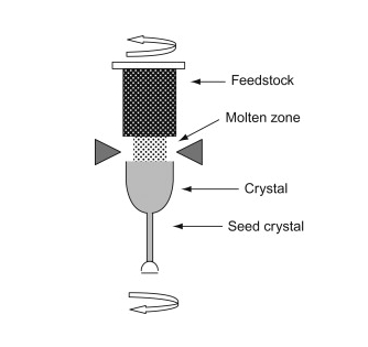
Advantages of the Float Zone Method:
High Purity: Since the silicon melt is not in contact with a crucible, the Float Zone method significantly reduces contamination, resulting in ultra-pure silicon crystals.
No Crucible Contact: The lack of contact with a crucible means that the crystal is free from impurities introduced by the container material, which is particularly important for high-purity applications.
Directional Solidification: The Float Zone method allows for precise control of the solidification process, ensuring the formation of high-quality crystals with minimal defects.
Conclusion
Monocrystalline silicon manufacturing is a vital process for producing high-quality materials used in the semiconductor and solar cell industries. The Czochralski, Kyropoulos, and Float Zone methods each offer unique advantages depending on the specific requirements of the application, such as crystal size, purity, and growth speed. As technology continues to advance, improvements in these crystal growth techniques will further enhance the performance of silicon-based devices in various high-tech fields.
Semicorex offers high-quality graphite parts for crystal growth process. If you have any inquiries or need additional details, please don't hesitate to get in touch with us.
Contact phone # +86-13567891907
Email: sales@semicorex.com