- English
- Español
- Português
- русский
- Français
- 日本語
- Deutsch
- tiếng Việt
- Italiano
- Nederlands
- ภาษาไทย
- Polski
- 한국어
- Svenska
- magyar
- Malay
- বাংলা ভাষার
- Dansk
- Suomi
- हिन्दी
- Pilipino
- Türkçe
- Gaeilge
- العربية
- Indonesia
- Norsk
- تمل
- český
- ελληνικά
- український
- Javanese
- فارسی
- தமிழ்
- తెలుగు
- नेपाली
- Burmese
- български
- ລາວ
- Latine
- Қазақша
- Euskal
- Azərbaycan
- Slovenský jazyk
- Македонски
- Lietuvos
- Eesti Keel
- Română
- Slovenski
- मराठी
- Srpski језик

4th Generation Semiconductors Gallium Oxide/β-Ga2O3
2024-07-05
The first generation of semiconductor materials is mainly represented by silicon (Si) and germanium (Ge), which began to rise in the 1950s. Germanium was dominant in the early days and was mainly used in low-voltage, low-frequency, medium-power transistors and photodetectors, but due to its poor high temperature resistance and radiation resistance, it was gradually replaced by silicon devices in the late 1960s. Silicon is still the main semiconductor material in the field of microelectronics due to its high technological maturity and cost advantages.
The second generation of semiconductor materials mainly include compound semiconductors such as gallium arsenide (GaAs) and indium phosphide (InP), which are widely used in high-performance microwaves, millimeter waves, optoelectronics, satellite communications and other fields. However, compared with silicon, its cost, technological maturity, and material properties have limited the development and popularization of second-generation semiconductor materials in cost-sensitive markets.
The representatives of the third generation of semiconductors mainly include gallium nitride (GaN) and silicon carbide (SiC), and everyone has been very familiar with these two materials in the past two years. SiC substrates were commercialized by Cree (later renamed Wolfspeed) in 1987, but it was not until Tesla's application in recent years that the large-scale commercialization of silicon carbide devices was truly promoted. From automotive main drives to photovoltaic energy storage to consumer white appliances, silicon carbide has entered our daily lives. The application of GaN is also popular in our daily mobile phones and computer charging devices. At present, most GaN devices are <650V and are widely used in the consumer field. The crystal growth speed of SiC is very slow (0.1-0.3mm per hour), and the crystal growth process has high technical requirements. In terms of cost and efficiency, it is far from comparable to silicon-based products.
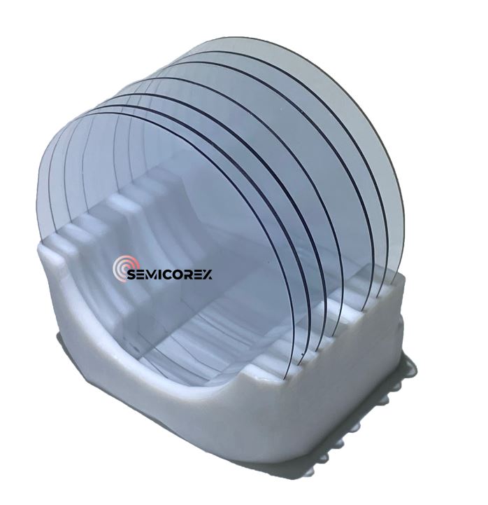
The fourth-generation semiconductors mainly include gallium oxide (Ga2O3), diamond (Diamond), and aluminum nitride (AlN). Among them, the difficulty of preparing the substrate of gallium oxide is lower than that of diamond and aluminum nitride, and its commercialization progress is the fastest and most promising. Compared with Si and third-generation materials, the fourth-generation semiconductor materials have higher band gaps and breakdown field strengths, and can provide power devices with higher withstand voltage.
One of the advantages of gallium oxide over SiC is that its single crystal can be grown by liquid phase method, such as the Czochralski method and guided mold method of traditional silicon rod production. Both methods first load high-purity gallium oxide powder into an iridium crucible and heat it to melt the powder.
The Czochralski method uses the seed crystal to contact the surface of the melt to start crystal growth. At the same time, the seed crystal is rotated and the seed crystal rod is slowly lifted to obtain a single crystal rod with uniform crystal structure.
The guided mold method requires a guide mold (made of iridium or other high-temperature resistant materials) to be installed above the crucible. When the guide mold is immersed in the melt, the melt is attracted to the upper surface of the mold by the template and siphon effect. The melt forms a thin film under the action of surface tension and diffuses to the surroundings. The seed crystal is placed down to contact the melt film, and the temperature gradient at the top of the mold is controlled to make the end face of the seed crystal crystallize a single crystal with the same structure as the seed crystal. Then the seed crystal is continuously lifted upward by the pulling mechanism. The seed crystal completes the preparation of the entire single crystal after shoulder release and equal diameter growth. The shape and size of the top of the mold determine the cross-sectional shape of the crystal grown by the guided mold method.