- English
- Español
- Português
- русский
- Français
- 日本語
- Deutsch
- tiếng Việt
- Italiano
- Nederlands
- ภาษาไทย
- Polski
- 한국어
- Svenska
- magyar
- Malay
- বাংলা ভাষার
- Dansk
- Suomi
- हिन्दी
- Pilipino
- Türkçe
- Gaeilge
- العربية
- Indonesia
- Norsk
- تمل
- český
- ελληνικά
- український
- Javanese
- فارسی
- தமிழ்
- తెలుగు
- नेपाली
- Burmese
- български
- ລາວ
- Latine
- Қазақша
- Euskal
- Azərbaycan
- Slovenský jazyk
- Македонски
- Lietuvos
- Eesti Keel
- Română
- Slovenski
- मराठी
- Srpski језик

Defect-Free Epitaxial Growth and Misfit Dislocations
2024-07-04
Defect-free epitaxial growth occurs when one crystal lattice has nearly identical lattice constants to another. Growth happens when lattice sites of the two lattices at the interface region are approximately matched, which is possible with a small lattice mismatch (less than 0.1%). This approximate matching is achieved even with elastic strain at the interface, where each atom is slightly displaced from its original position in the boundary layer. While a small amount of strain is tolerable for thin layers and even desirable for quantum well lasers, the strain energy stored in the crystal is generally lowered by the formation of misfit dislocations, which involve a missing row of atoms in one lattice.
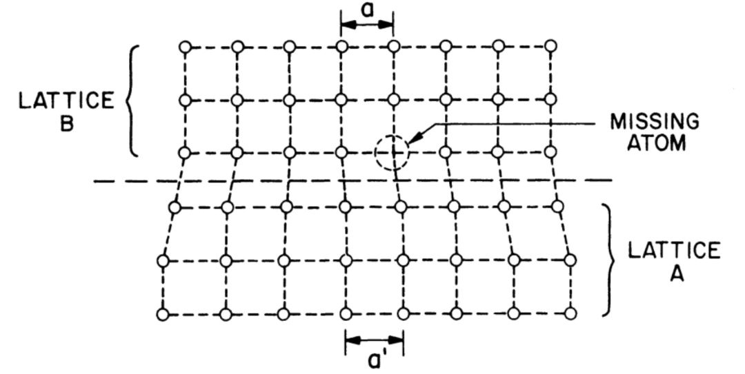
The figure above illustrates a schematic of a misfit dislocation formed during epitaxial growth on a cubic (100) plane, where the two semiconductors have slightly different lattice constants. If a is the lattice constant of the substrate and a’ = a − Δa is that of the growing layer, then the spacing between each missing row of atoms is approximately:
L ≈ a<sup>2</sup>/Δa
At the interface of the two lattices, the missing rows of atoms exist along two perpendicular directions. The spacing between rows along the principal crystal axes, such as [100], is approximately given by the above formula.
This type of defect at the interface is termed a dislocation. Since it arises from the lattice mismatch (or misfit), it is called a misfit dislocation, or simply a dislocation.
In the vicinity of misfit dislocations, the lattice is imperfect with many dangling bonds, which can lead to non-radiative recombination of electrons and holes. Therefore, for high-quality optoelectronic device fabrication, misfit dislocation-free layers are required.
The generation of misfit dislocations depends on the lattice mismatch and the thickness of the epitaxial layer grown. If the lattice mismatch Δa/a is in the range of -5 × 10<sup>-3</sup> to 5 × 10<sup>-3</sup>, then no misfit dislocations are formed in InGaAsP-InP double heterostructure layers (0.4 µm thick) grown on (100) InP.
The occurrence of dislocations as a function of lattice mismatch for different thicknesses of InGaAs layers grown at 650°C on (100) InP is shown in the figure below.
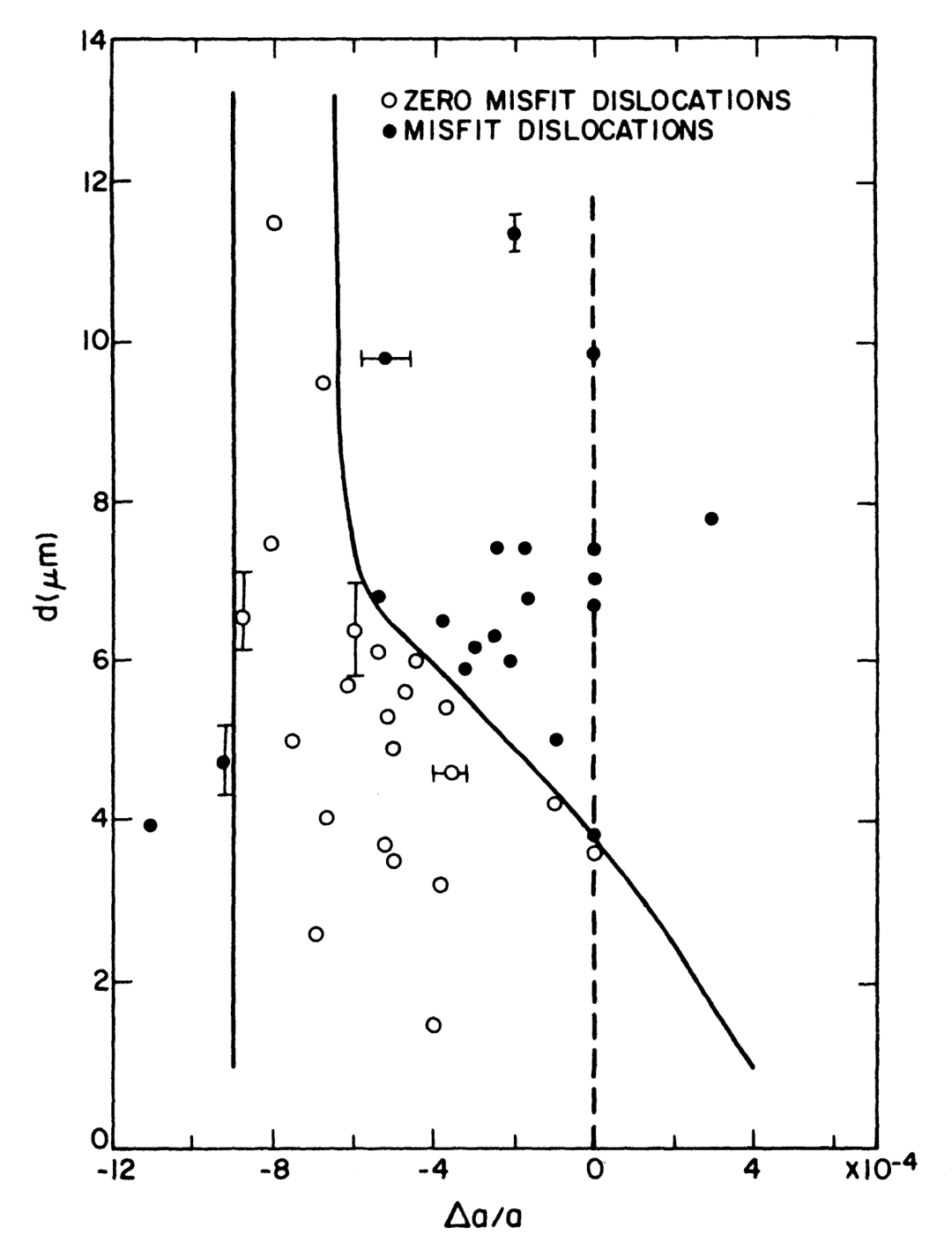
This figure illustrates the occurrence of misfit dislocations as a function of lattice mismatch for different thicknesses of InGaAs layers grown by LPE on (100) InP. No misfit dislocations are observed in the region bounded by solid lines.
As shown in the figure above, the solid line represents the boundary where no dislocations were observed. For the growth of thick dislocation-free InGaAs layers, the tolerable room-temperature lattice mismatch is found to be between -6.5 × 10<sup>-4</sup> and -9 × 10<sup>-4</sup>.
This negative lattice mismatch arises because of the difference in the thermal expansion coefficients of InGaAs and InP; a perfectly matched layer at the growth temperature of 650°C will have a negative room-temperature lattice mismatch.
Since the misfit dislocations are formed around the growth temperature, lattice matching at the growth temperature is important for the growth of dislocation-free layers.**
Previous:Oxidation Process