- English
- Español
- Português
- русский
- Français
- 日本語
- Deutsch
- tiếng Việt
- Italiano
- Nederlands
- ภาษาไทย
- Polski
- 한국어
- Svenska
- magyar
- Malay
- বাংলা ভাষার
- Dansk
- Suomi
- हिन्दी
- Pilipino
- Türkçe
- Gaeilge
- العربية
- Indonesia
- Norsk
- تمل
- český
- ελληνικά
- український
- Javanese
- فارسی
- தமிழ்
- తెలుగు
- नेपाली
- Burmese
- български
- ລາວ
- Latine
- Қазақша
- Euskal
- Azərbaycan
- Slovenský jazyk
- Македонски
- Lietuvos
- Eesti Keel
- Română
- Slovenski
- मराठी
- Srpski језик

Ion Implant and Diffusion Process
2024-06-21
Ion implantation is a method of semiconductor doping and one of the main processes in semiconductor manufacturing.
Why doping?
Pure silicon/intrinsic silicon has no free carriers (electrons or holes) inside and has poor conductivity. In semiconductor technology, doping is to intentionally add a very small amount of impurity atoms to intrinsic silicon to change the electrical properties of silicon, making it more conductive and thus capable of being used to manufacture various semiconductor devices. Doping can be n-type doping or p-type doping. n-type doping: achieved by doping pentavalent elements (such as phosphorus, arsenic, etc.) into silicon; p-type doping: achieved by doping trivalent elements (such as boron, aluminum, etc.) into silicon. Doping methods usually include thermal diffusion and ion implantation.
Thermal diffusion method
Thermal diffusion is to migrate impurity elements into silicon by heating. The migration of this substance is caused by high-concentration impurity gas toward low-concentration silicon substrate, and its migration mode is determined by concentration difference, temperature, and diffusion coefficient. Its doping principle is that at high temperature, atoms in the silicon wafer and atoms in the doping source will obtain enough energy to move. The atoms of the doping source are first adsorbed on the surface of the silicon wafer, and then these atoms dissolve into the surface layer of the silicon wafer. At high temperatures, doping atoms diffuse inward through the lattice gaps of the silicon wafer or replace the positions of silicon atoms. Eventually, the doping atoms reach a certain distribution balance inside the wafer. The thermal diffusion method has low costs and mature processes. However, it also has some limitations, such as the control of doping depth and concentration is not as precise as ion implantation, and the high temperature process may introduce lattice damage, etc.
Ion implantation:
It refers to ionizing the doping elements and forming an ion beam, which is accelerated to a certain energy (keV~MeV level) through high voltage to collide with the silicon substrate. The doping ions are physically implanted into the silicon to change the physical properties of the doped area of the material.
Advantages of ion implantation:
It is a low-temperature process, the implantation amount/doping amount can be monitored, and the impurity content can be precisely controlled; the implantation depth of impurities can be precisely controlled; the impurity uniformity is good; in addition to the hard mask, photoresist can also be used as a mask; it is not limited by compatibility (the dissolution of impurity atoms in silicon crystals due to thermal diffusion doping is limited by the maximum concentration, and there is a balanced dissolution limit, while ion implantation is a non-equilibrium physical process. Impurity atoms are injected into silicon crystals with high energy, which can exceed the natural dissolution limit of impurities in silicon crystals. One is to moisten things silently, and the other is to force the bow.)
Principle of ion implantation:
First, impurity gas atoms are hit by electrons in the ion source to generate ions. The ionized ions are extracted by the suction component to form an ion beam. After magnetic analysis, the ions with different mass-to-charge ratios are deflected (because the ion beam formed in the front contains not only the ion beam of the target impurity, but also the ion beam of other material elements, which must be filtered out), and the pure impurity element ion beam that meets the requirements is separated, and then it is accelerated by high voltage, the energy is increased, and it is focused and electronically scanned, and finally hit at the target position to achieve implantation.
The impurities implanted by ions are electrically inactive without treatment, so after ion implantation, they are generally subjected to high-temperature annealing to activate the impurity ions, and high temperature can repair the lattice damage caused by ion implantation.
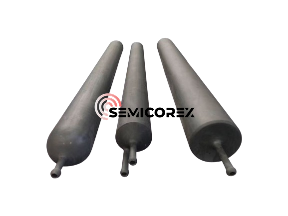
Semicorex offers high-quality SiC parts in ion implant and diffusion process. If you have any inquiries or need additional details, please don't hesitate to get in touch with us.
Contact phone # +86-13567891907
Email: sales@semicorex.com