
- English
- Español
- Português
- русский
- Français
- 日本語
- Deutsch
- tiếng Việt
- Italiano
- Nederlands
- ภาษาไทย
- Polski
- 한국어
- Svenska
- magyar
- Malay
- বাংলা ভাষার
- Dansk
- Suomi
- हिन्दी
- Pilipino
- Türkçe
- Gaeilge
- العربية
- Indonesia
- Norsk
- تمل
- český
- ελληνικά
- український
- Javanese
- فارسی
- தமிழ்
- తెలుగు
- नेपाली
- Burmese
- български
- ລາວ
- Latine
- Қазақша
- Euskal
- Azərbaycan
- Slovenský jazyk
- Македонски
- Lietuvos
- Eesti Keel
- Română
- Slovenski
- मराठी
- Srpski језик

Challenges of Ion Implantation Technology in SiC and GaN Power Devices
2024-06-21
Wide bandgap (WBG) semiconductors such as Silicon Carbide (SiC) and Gallium Nitride (GaN) are expected to play an increasingly important role in power electronic devices. They offer several advantages over traditional Silicon (Si) devices, including higher efficiency, power density, and switching frequency. Ion implantation is the primary method for achieving selective doping in Si devices. However, there are some challenges when applying it to wide bandgap devices. In this article, we will focus on some of these challenges and summarize their potential applications in GaN power devices.
01
Several factors determine the practical use of dopant materials in semiconductor device manufacturing:
Low ionization energy in the occupied lattice sites. Si has ionizable shallow donors (for n-type doping) and acceptors (for p-type doping) elements. The deeper energy levels within the bandgap result in poor ionization, especially at room temperature, leading to lower conductivity for a given dose.Source materials ionizable and injectable in commercial ion implanters. Solid and gas source materials compounds can be used, and their practical use depends on temperature stability, safety, ion generation efficiency, ability to produce unique ions for mass separation, and achieve the desired energy implantation depth.
Source materials ionizable and injectable in commercial ion implanters. Solid and gas source materials compounds can be used, and their practical use depends on temperature stability, safety, ion generation efficiency, ability to produce unique ions for mass separation, and achieve the desired energy implantation depth.
Table 1: Common dopant species used in SiC and GaN power devices
Diffusion rates within the implanted material. High diffusion rates under normal post-implant annealing conditions can lead to uncontrolled junctions and dopant diffusion into undesired areas of the device, resulting in degraded device performance.
Activation and damage recovery. Dopant activation involves generating vacancies at high temperatures, allowing the implanted ions to move from interstitial positions to substitutional lattice positions. Damage recovery is crucial for repairing amorphization and crystal defects created during the implantation process.
Table 1 lists some commonly used dopant species and their ionization energies in SiC and GaN device manufacturing.
While n-type doping in both SiC and GaN is relatively straightforward with shallow dopants, a key challenge in creating p-type doping through ion implantation is the high ionization energy of available elements.
02
Some key implantation and annealing characteristics of GaN include:
Unlike SiC, there is no significant advantage in using hot implantation compared to room temperature.
For GaN, the commonly used n-type dopant Si can be ambipolar, exhibiting n-type and/or p-type behavior depending on its occupation site. This may depend on GaN growth conditions and lead to partial compensation effects.
P-doping of GaN is more challenging due to the high background electron concentration in undoped GaN, requiring high levels of Magnesium (Mg) p-type dopant to convert the material into p-type. However, high doses result in high levels of defects, leading to carrier capture and compensation at deeper energy levels, resulting in poor dopant activation.
GaN decomposes at temperatures higher than 840°C under atmospheric pressure, leading to N loss and the formation of Ga droplets on the surface. Various forms of rapid thermal annealing (RTA) and protective layers such as SiO2 have been employed. Annealing temperatures are typically lower (<1500°C) compared to those used for SiC. Several methods such as high-pressure, multi-cycle RTA, microwave, and laser annealing have been attempted. Nevertheless, achieving p+ implantation contacts remains a challenge.
03
In vertical Si and SiC power devices, a common approach for edge termination is to create a p-type doping ring through ion implantation. If selective doping can be achieved, it would also facilitate the formation of vertical GaN devices. Magnesium (Mg) dopant ion implantation faces several challenges, and some of them are listed below.
1. High ionization potential (as shown in Table 1).
2. Defects generated during the implantation process may lead to the formation of permanent clusters, causing deactivation.
3. High temperatures (>1300°C) are required for activation. This exceeds the decomposition temperature of GaN, necessitating special methods. One successful example is the use of ultra-high pressure annealing (UHPA) with N2 pressure at 1 GPa. Annealing at 1300-1480°C achieves over 70% activation and exhibits good surface carrier mobility.
4. At these high temperatures, magnesium diffusion interacts with point defects in the damaged regions, which can result in graded junctions. Control of Mg distribution in p-GaN e-mode HEMTs is a key challenge, even when employing MOCVD or MBE growth processes.
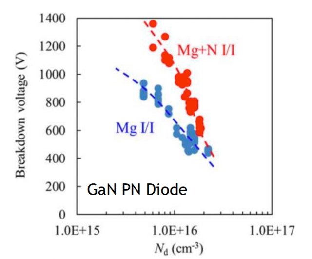
Figure 1: Increased pn junction breakdown voltage through Mg/N co-implantation
The co-implantation of nitrogen (N) with Mg has been shown to improve the activation of Mg dopants and suppress diffusion. The improved activation is attributed to the inhibition of vacancy agglomeration by N implantation, which facilitates the recombination of these vacancies at annealing temperatures above 1200°C. Additionally, the vacancies generated by N implantation limit the diffusion of Mg, resulting in steeper junctions. This concept has been used to manufacture vertical planar GaN MOSFETs through a full ion implantation process. The specific on-resistance (RDSon) of the 1200V device reached an impressive 0.14 Ohms-mm2. If this process can be utilized for large-scale manufacturing, it could be cost-effective and follow the common process flow used in Si and SiC planar vertical power MOSFET fabrication. As shown in Figure 1, the use of co-implantation methods accelerates pn junction breakdown.
04
Due to the aforementioned issues, p-GaN doping is typically grown rather than implanted in p-GaN e-mode high electron mobility transistors (HEMTs). One application of ion implantation in HEMTs is lateral device isolation. Various implant species, such as hydrogen (H), N, iron (Fe), argon (Ar), and oxygen (O), have been attempted. The mechanism is mainly related to trap formation associated with damage. The advantage of this method compared to mesa etch isolation processes is device flatness. Figure 2-1 describes the relationship between the achieved isolation layer resistance and the annealing temperature after implantation. As shown in the figure, resistances of over 107 Ohms/sq can be achieved.
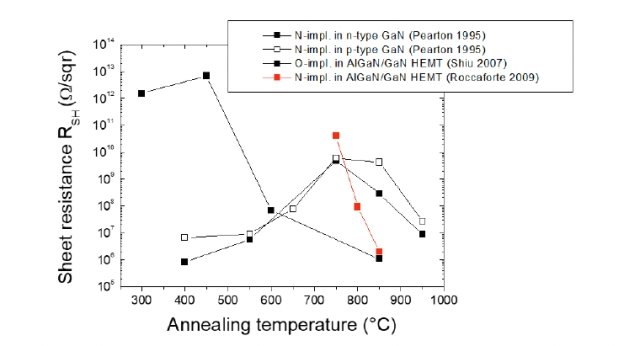
Figure 2: Relationship between the isolation layer resistance and the annealing temperature after various GaN isolation implantations
Although several studies have been conducted on creating n+ Ohmic contacts in GaN layers using silicon (Si) implantation, practical implementation can be challenging due to high impurity concentrations and resulting lattice damage. One motivation for using Si implantation is to achieve low-resistance contacts through Si CMOS compatible processes or subsequent post-metal alloy processes without the use of gold (Au).
05
In HEMTs, low-dose fluorine (F) implantation has been used to increase the breakdown voltage (BV) of devices by leveraging F’s strong electronegativity. The formation of a negatively charged region on the backside of the 2-DEG electron gas suppresses the injection of electrons into high-field regions.
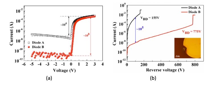
Figure 3: (a) Forward characteristics and (b) reverse IV of vertical GaN SBD showing improvement after F implantation
Another interesting application of ion implantation in GaN is the use of F implantation in vertical Schottky Barrier Diodes (SBDs). Here, F implantation is performed on the surface next to the top anode contact to create a high-resistance edge termination region. As shown in Figure 3, the reverse current is reduced by five orders of magnitude, while BV is increased.**


