
- English
- Español
- Português
- русский
- Français
- 日本語
- Deutsch
- tiếng Việt
- Italiano
- Nederlands
- ภาษาไทย
- Polski
- 한국어
- Svenska
- magyar
- Malay
- বাংলা ভাষার
- Dansk
- Suomi
- हिन्दी
- Pilipino
- Türkçe
- Gaeilge
- العربية
- Indonesia
- Norsk
- تمل
- český
- ελληνικά
- український
- Javanese
- فارسی
- தமிழ்
- తెలుగు
- नेपाली
- Burmese
- български
- ລາວ
- Latine
- Қазақша
- Euskal
- Azərbaycan
- Slovenský jazyk
- Македонски
- Lietuvos
- Eesti Keel
- Română
- Slovenski
- मराठी
- Srpski језик

Introduction to Third-Generation Semiconductors: GaN and Related Epitaxial Technologies
1. Third-Generation Semiconductors
(1) First-Generation Semiconductors
The first-generation semiconductor technology is based on materials like silicon (Si) and germanium (Ge). These materials laid the foundation for transistor and integrated circuit (IC) technology, which in turn established the basis of the 20th-century electronics industry.
The second-generation semiconductor materials primarily include gallium arsenide (GaAs), indium phosphide (InP), gallium phosphide (GaP), indium arsenide (InAs), aluminum arsenide (AlAs), and their ternary compounds. These materials form the backbone of the optoelectronic information industry, which has led to the development of lighting, display, laser, photovoltaic, and other related industries. They are widely used in contemporary information technology and optoelectronic display industries.
(3) Third-Generation Semiconductors
Representative materials of third-generation semiconductors include gallium nitride (GaN) and silicon carbide (SiC). Due to their wide bandgap, high electron saturation drift velocity, high thermal conductivity, and large breakdown electric fields, these materials are ideal for high power density, high frequency, and low-loss electronic devices. SiC power devices have high energy density, low energy consumption, and small size, making them suitable for applications in electric vehicles, photovoltaics, rail transportation, and big data sectors. GaN RF devices feature high frequency, high power, wide bandwidth, low power consumption, and small size, which are advantageous for 5G communications, the Internet of Things (IoT), and military radar applications. Additionally, GaN-based power devices are now widely used in low-voltage applications. Emerging gallium oxide (Ga2O3) materials also show potential for complementing existing SiC and GaN technologies, especially in low-frequency, high-voltage applications.
Compared to second-generation semiconductor materials, third-generation materials possess wider bandgaps (typical Si has a bandgap of about 1.1 eV, GaAs about 1.42 eV, while GaN exceeds 2.3 eV), stronger radiation resistance, higher electric field breakdown performance, and better high-temperature endurance. These characteristics make third-generation semiconductor materials particularly suitable for radiation-resistant, high-frequency, high-power, and high-integration density electronic devices. They are making significant strides in microwave RF devices, LEDs, lasers, and power devices, and show promising prospects in mobile communications, smart grids, rail transportation, electric vehicles, consumer electronics, and ultraviolet and blue-green light devices[1].
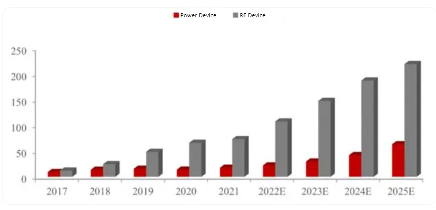
Figure 1: Market Size and Forecast of GaN Power Devices
2. Structure and Characteristics of GaN
Gallium Nitride (GaN) is a direct bandgap semiconductor with a bandgap of approximately 3.26 eV at room temperature in its wurtzite structure. GaN primarily exists in three crystalline structures: wurtzite, zincblende, and rock-salt. The wurtzite structure is the most stable among these. Figure 2 displays the hexagonal wurtzite structure of GaN. In the wurtzite structure, GaN belongs to the hexagonal close-packed configuration. Each unit cell contains 12 atoms, including 6 nitrogen (N) atoms and 6 gallium (Ga) atoms. Each Ga (N) atom is bonded to 4 nearest N (Ga) atoms, forming a stacking sequence along the [0001] direction in an ABABAB… pattern[2].
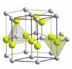
Figure 2: Wurtzite Structure of GaN Unit Cell
At first glance, homoepitaxy on GaN substrates appears to be the optimal choice for GaN epitaxy. However, due to the high bond energy of GaN, at its melting point (2500°C), the corresponding decomposition pressure is approximately 4.5 GPa. Below this pressure, GaN does not melt but directly decomposes. This makes traditional substrate preparation techniques, such as the Czochralski method, unsuitable for the preparation of GaN single crystal substrates. Consequently, GaN substrates are difficult to mass-produce and are costly. Therefore, the commonly used substrates for GaN epitaxy include Si, SiC, and sapphire[3].
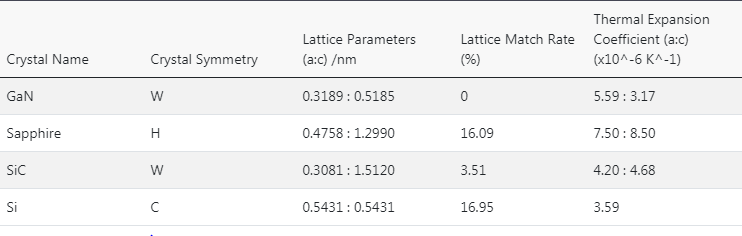
Figure 3: Parameters of GaN and Common Substrate Materials
(1) GaN Epitaxy on Sapphire
Sapphire is chemically stable, inexpensive, and has a high degree of maturity in mass production, making it one of the earliest and most widely used substrate materials in semiconductor device engineering. As a common substrate for GaN epitaxy, sapphire substrates need to address the following key issues:
✔ High Lattice Mismatch: The lattice mismatch between sapphire (Al2O3) and GaN is significant (approximately 15%), leading to a high defect density at the interface between the epitaxial layer and the substrate. To mitigate this adverse effect, the substrate must undergo complex pre-processing before the epitaxial process begins. This includes thorough cleaning to remove contaminants and residual polishing damage, creating steps and step surface structures, surface nitridation to alter the wetting properties of the epitaxial layer, and finally depositing a thin AlN buffer layer (typically 10-100 nm thick) followed by low-temperature annealing to prepare for the final epitaxial growth. Despite these measures, the dislocation density in GaN epitaxial films grown on sapphire substrates remains high (~10^10 cm^-2) compared to homoepitaxy on silicon or GaAs (dislocation density of 0 to 102-104 cm^-2). High defect densities reduce carrier mobility, shorten minority carrier lifetimes, and decrease thermal conductivity, all of which impair device performance[4].
✔ Thermal Expansion Coefficient Mismatch: Sapphire has a greater thermal expansion coefficient than GaN, resulting in biaxial compressive stress within the epitaxial layer as it cools from deposition temperature to room temperature. For thicker epitaxial films, this stress may lead to film or even substrate cracking.
✔ Poor Thermal Conductivity: Compared to other substrates, sapphire has a lower thermal conductivity (~0.25 Wcm^-1K^-1 at 100°C), which is disadvantageous for heat dissipation.
✔ Low Electrical Conductivity: The poor electrical conductivity of sapphire hinders its integration and application with other semiconductor devices.
Despite the high defect density in GaN epitaxial layers grown on sapphire, its optical and electronic performance in GaN-based blue-green LEDs does not appear significantly diminished. Therefore, sapphire substrates remain common for GaN-based LEDs. However, as more GaN devices such as lasers and other high-density power devices develop, the inherent limitations of sapphire substrates become increasingly apparent.
(2) GaN Epitaxy on SiC
Compared to sapphire, SiC substrates (4H- and 6H-polytypes) have a smaller lattice mismatch with GaN epitaxial layers (3.1% along the [0001] direction), higher thermal conductivity (approximately 3.8 Wcm^-1K^-1), and electrical conductivity that allows for backside electrical contacts, simplifying device structures. These advantages draw increasing numbers of researchers to explore GaN epitaxy on SiC substrates. However, direct growth of GaN epitaxial layers on SiC substrates also faces several challenges:
✔ Surface Roughness: SiC substrates have much higher surface roughness than sapphire substrates (0.1 nm RMS for sapphire, 1 nm RMS for SiC). The high hardness and poor machinability of SiC contribute to this roughness and residual polishing damage, which are sources of defects in GaN epitaxial layers.
✔ High Threading Dislocation Density: SiC substrates have high threading dislocation densities (103-104 cm^-2), which can propagate into the GaN epitaxial layer and degrade device performance.
✔ Stacking Faults: The atomic arrangement on the substrate surface can induce stacking faults (BSFs) in the GaN epitaxial layers. Multiple possible atomic arrangements on the SiC substrate lead to non-uniform initial atomic stacking sequences in the GaN layer, increasing the likelihood of stacking faults. BSFs along the c-axis introduce built-in electric fields, causing carrier separation and leakage issues in devices.
✔ Thermal Expansion Coefficient Mismatch: The thermal expansion coefficient of SiC is smaller than that of AlN and GaN, leading to thermal stress accumulation between the epitaxial layer and substrate during cooling. Waltereit and Brand’s research suggests that this issue can be mitigated by growing the GaN epitaxial layer on a thin, coherently strained AlN nucleation layer.
✔ Poor Wetting of Ga Atoms: Direct growth of GaN on SiC surfaces is difficult due to poor wetting of Ga atoms. GaN tends to grow in a 3D island mode, introducing buffer layers is a common solution to improve the quality of epitaxial materials. Introducing AlN or AlxGa1-xN buffer layers can improve wetting on the SiC surface, promoting 2D growth of the GaN epitaxial layer and acting to modulate stress and block substrate defects from propagating into the GaN layer.
✔ High Cost and Limited Supply: SiC substrate preparation technology is immature, leading to high substrate costs and limited supply from few vendors.
Research by Torres et al. indicates that pre-etching SiC substrates with H2 at high temperatures (1600°C) creates more orderly step structures, resulting in higher-quality AlN epitaxial films compared to those directly grown on untreated substrates. Xie and his team also demonstrated that etching pretreatment of SiC substrates significantly improves the surface morphology and crystal quality of GaN epitaxial layers. Smith et al. found that threading dislocations from the substrate/buffer layer and buffer layer/epitaxial layer interfaces are related to substrate flatness[5].
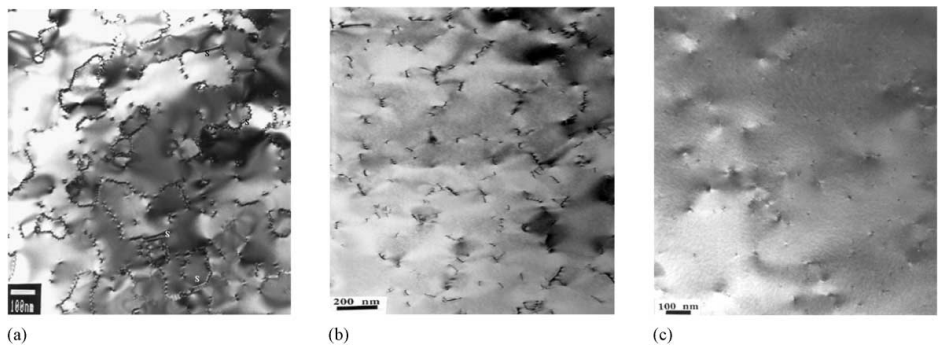
Figure 4: TEM Morphology of GaN Epitaxial Layers Grown on (0001) Face of 6H-SiC Substrates Under Different Surface Treatments: (a) Chemical Cleaning; (b) Chemical Cleaning + Hydrogen Plasma Treatment; © Chemical Cleaning + Hydrogen Plasma Treatment + 1300°C Hydrogen Thermal Treatment for 30 min
(3) GaN Epitaxy on Si
Compared to SiC and sapphire substrates, silicon substrates boast mature preparation processes, stable large-size substrate supply, cost-effectiveness, and excellent thermal and electrical conductivity. Additionally, the mature silicon electronic device technology offers the potential for perfect integration of optoelectronic GaN devices with silicon electronic devices, making GaN epitaxy on silicon highly attractive. However, the significant lattice constant mismatch between Si substrates and GaN materials presents several challenges.
✔ Interface Energy Issues: When GaN is grown on Si substrates, the Si surface first forms an amorphous SiNx layer, which is detrimental to high-density GaN nucleation. Additionally, Si surfaces initially react with Ga, causing surface corrosion, and at high temperatures, Si surface decomposition can diffuse into the GaN epitaxial layer, forming black silicon spots.
✔ Lattice Mismatch: The large lattice constant mismatch (~17%) between GaN and Si results in high-density threading dislocations, significantly reducing the quality of the epitaxial layer.
✔ Thermal Expansion Coefficient Mismatch: GaN has a larger thermal expansion coefficient than Si (GaN ~5.6×10^-6 K^-1, Si ~2.6×10^-6 K^-1), which may cause cracks in the GaN epitaxial layer during cooling from epitaxial growth temperature to room temperature.
✔ High-Temperature Reactions: Si reacts with NH3 at high temperatures, forming polycrystalline SiNx. AlN cannot preferentially nucleate on polycrystalline SiNx, leading to highly disoriented GaN growth with very high defect densities, making it challenging to form single-crystal GaN epitaxial layers[6].
To address the large lattice mismatch, researchers have attempted to introduce materials such as AlAs, GaAs, AlN, GaN, ZnO, and SiC as buffer layers on Si substrates. To prevent the formation of polycrystalline SiNx and reduce its adverse effects on the crystal quality of GaN/AlN/Si (111), TMAl is usually introduced before epitaxial growth of the AlN buffer layer to prevent NH3 from reacting with the exposed Si surface. Additionally, techniques such as patterned substrates are utilized to improve epitaxial layer quality. These developments help suppress the formation of SiNx at the epitaxial interface, promote 2D growth of the GaN epitaxial layer, and enhance growth quality. Introducing AlN buffer layers compensates for tensile stress caused by differences in thermal expansion coefficients, preventing cracks in the GaN layer on silicon substrates. Krost’s research indicates a positive correlation between AlN buffer layer thickness and reduced strain, allowing growth of over 6 μm thick epitaxial layers on silicon substrates without cracking, through appropriate growth schemes.
Thanks to extensive research efforts, the quality of GaN epitaxial layers grown on silicon substrates has improved significantly. Field-effect transistors, Schottky barrier ultraviolet detectors, blue-green LEDs, and ultraviolet lasers have all made significant progress.
In conclusion, the common GaN epitaxial substrates are all heteroepitaxial, facing varying degrees of lattice mismatch and thermal expansion coefficient differences. Homoepitaxial GaN substrates are limited by immature technology, high production costs, small substrate sizes, and suboptimal quality, making the development of new GaN epitaxial substrates and improvement of epitaxial quality critical factors for further industry advancement.
4. Common Methods for GaN Epitaxy
(1) MOCVD (Metal-Organic Chemical Vapor Deposition)
While homoepitaxy on GaN substrates appears to be the optimal choice for GaN epitaxy, Metal-Organic Chemical Vapor Deposition (MOCVD) offers significant advantages. Using trimethylgallium and ammonia as precursors, and hydrogen as the carrier gas, MOCVD typically operates at growth temperatures around 1000-1100°C. The growth rate of MOCVD is in the range of several micrometers per hour. This method can produce atomically sharp interfaces, making it ideal for growing heterojunctions, quantum wells, and superlattices. Its relatively high growth speed, excellent uniformity, and suitability for large-area and multi-wafer growth make it a standard method for industrial production.
(2) MBE (Molecular Beam Epitaxy)
In Molecular Beam Epitaxy (MBE), elemental sources are used for gallium, and active nitrogen is generated via RF plasma from nitrogen gas. Compared to MOCVD, MBE operates at significantly lower growth temperatures, around 350-400°C. This lower temperature can avoid some of the contamination issues that may arise in high-temperature environments. MBE systems work under ultra-high vacuum conditions, allowing for the integration of more in-situ monitoring techniques. However, the growth rate and production capacity of MBE cannot match that of MOCVD, making it more suitable for research applications[7].

Figure 5: (a) Schematic of Eiko-MBE (b) Schematic of MBE Main Reaction Chamber
(3) HVPE (Hydride Vapor Phase Epitaxy)
Hydride Vapor Phase Epitaxy (HVPE) utilizes GaCl3 and NH3 as precursors. Detchprohm et al. used this method to grow several hundred micrometers thick GaN epitaxial layers on sapphire substrates. In their experiments, a ZnO buffer layer was grown between the sapphire substrate and the epitaxial layer, allowing the epitaxial layer to be peeled off from the substrate surface. Compared to MOCVD and MBE, the primary advantage of HVPE is its high growth rate, making it suitable for producing thick layers and bulk materials. However, when the epitaxial layer thickness exceeds 20μm, layers grown by HVPE are prone to cracking.
Akira USUI introduced patterned substrate technology based on the HVPE method. Initially, a thin GaN epitaxial layer, 1-1.5μm thick, was grown on a sapphire substrate using MOCVD. This layer consisted of a 20nm thick low-temperature GaN buffer layer and a high-temperature GaN layer. Subsequently, at 430°C, a layer of SiO2 was deposited on the epitaxial layer’s surface, and window stripes were created on the SiO2 film through photolithography. The stripe spacing was 7μm, with mask widths ranging from 1μm to 4μm. This modification enabled them to produce GaN epitaxial layers on 2-inch diameter sapphire substrates, which remained crack-free and mirror-smooth even when the thickness increased to tens or even hundreds of micrometers. The defect density was reduced from the traditional HVPE method’s 109-1010 cm^-2 to approximately 6×10^7 cm^-2. They also noted that the sample surface became rough when the growth rate exceeded 75μm/h[8].
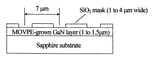
Figure 6: Schematic of Patterned Substrate
5. Summary and Outlook
The immense market demand will undoubtedly drive significant advancements in GaN-related industries and technologies. As the industrial chain for GaN matures and improves, current challenges in GaN epitaxy will eventually be mitigated or overcome. Future developments will likely introduce new epitaxial techniques and superior substrate options. This progress will enable the selection of the most suitable epitaxial technology and substrate based on the characteristics of different application scenarios, leading to the production of highly competitive, customized products.**
References:
[1] 「关注」半导体材料-氮化镓 (baidu.com)
[2]唐林江,万成安,张明华,李莹,宽禁带半导体材料SiC和GaN的研究现状,军民两用技术与产品,2020年3月,总第437期,21-28.
[3]王欢,田野,硅衬底氮化镓大失配应力调控方法研究,科技创新与应用,2023年3期
[4]L.Liu, J.H.Edgar, Substrates for gallium nitride epitaxy,Materialss Science and Engineering R, 37(2002) 61-127.
[5]P.Ruterana, Philippe Vermaut, G.Nouet, A.Salvador, H.Morkoc, Surface treatment and layer structure in 2H-GaN growth on the (0001)Si surface of 6H-SiC by MBE, MRS Internet J.Nitride Semicond. Res.2(1997)42.
[6]M.A.Sanchez-Garcia, F.B. Naranjo, J.L.Pau, A.Jimenez, E.Calleja, E.Munoz,Ultraviolet electroluminescence in GaN/AlGaN single-heterojunction light-emitting diodes grown on Si(111),Journal of Applied Physics 87,1569(2000).
[7]Xinqiang Wang, Akihiko Yoshikawa, Molecular beam epitaxy growth of GaN, AlN and InN, Progress in Crystal Growth and Characterization of Materials 48/49 (2004) 42-103.
[8]Akira Usui,Haruo Sunakawa,Akira Sakai and A. atsushi Yamaguchi, Thick GaN epitaxial growth with low dislocation density by hydride vapor phase epitaxy, Jpn. J. Appl. Phys. Vol. 36 (1997) pp.899-902.


