- English
- Español
- Português
- русский
- Français
- 日本語
- Deutsch
- tiếng Việt
- Italiano
- Nederlands
- ภาษาไทย
- Polski
- 한국어
- Svenska
- magyar
- Malay
- বাংলা ভাষার
- Dansk
- Suomi
- हिन्दी
- Pilipino
- Türkçe
- Gaeilge
- العربية
- Indonesia
- Norsk
- تمل
- český
- ελληνικά
- український
- Javanese
- فارسی
- தமிழ்
- తెలుగు
- नेपाली
- Burmese
- български
- ລາວ
- Latine
- Қазақша
- Euskal
- Azərbaycan
- Slovenský jazyk
- Македонски
- Lietuvos
- Eesti Keel
- Română
- Slovenski
- मराठी
- Srpski језик

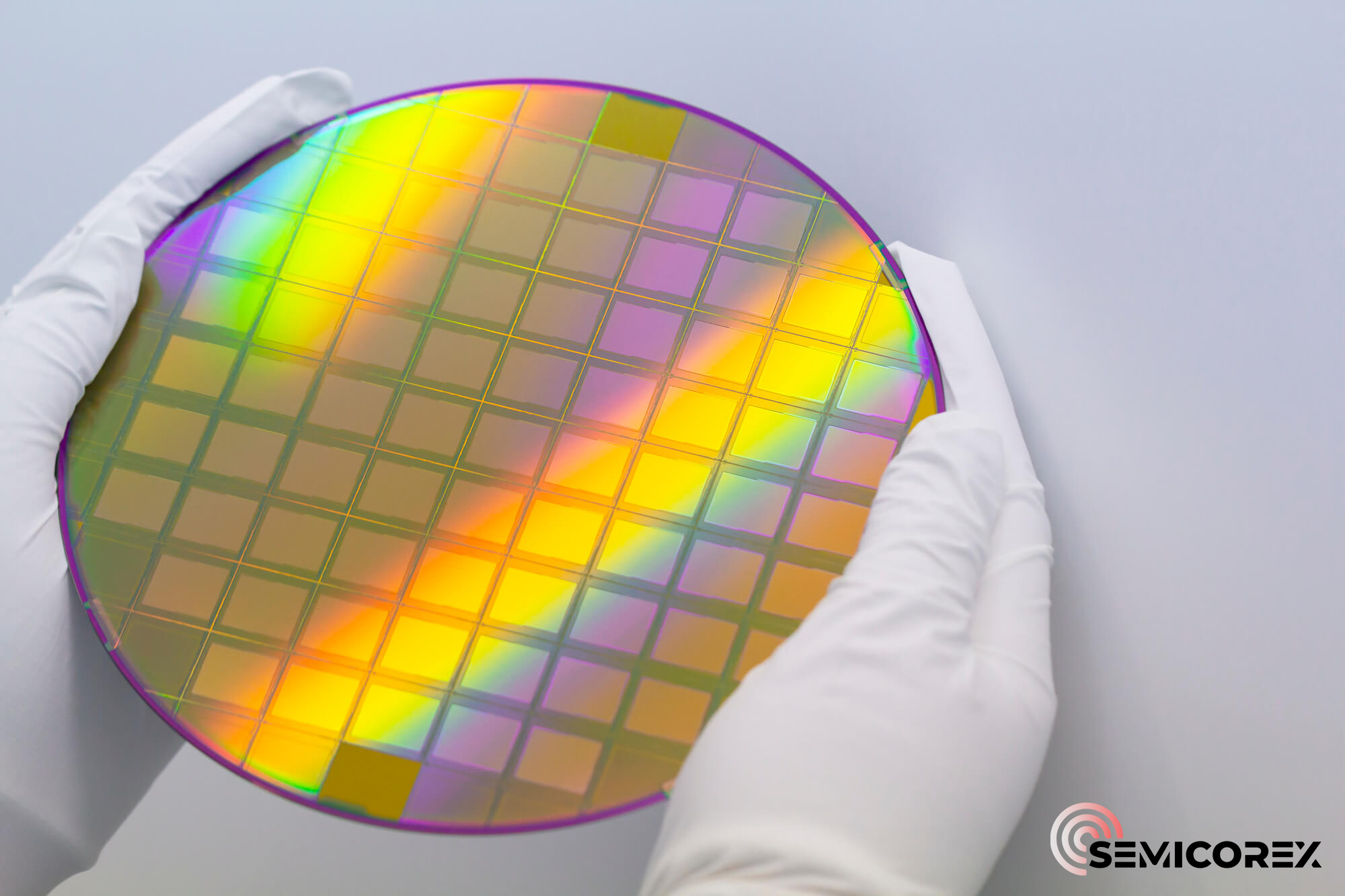
Substrate vs. Epitaxy: Key Roles in Semiconductor Manufacturing
2024-05-29
I. Semiconductor Substrate
A semiconductor substrate forms the foundation of semiconductor devices, providing a stable crystalline structure upon which the necessary material layers can grow. Substrates can be monocrystalline, polycrystalline, or even amorphous, depending on application requirements. The choice of substrate is crucial for the performance of semiconductor devices.
(1) Types of Substrates
Depending on the material, common semiconductor substrates include silicon-based, sapphire-based, and quartz-based substrates. Silicon-based substrates are widely used due to their cost-effectiveness and excellent mechanical properties. Monocrystalline silicon substrates, known for their high crystal quality and uniform doping, are extensively employed in integrated circuits and solar cells. Sapphire substrates, appreciated for their superior physical properties and high transparency, are used in the manufacture of LEDs and other optoelectronic devices. Quartz substrates, valued for their thermal and chemical stability, find applications in high-end devices.
(2) Functions of Substrates
Substrates primarily serve two functions in semiconductor devices: mechanical support and thermal conduction. As mechanical supports, substrates provide physical stability, maintaining the shape and dimensional integrity of the devices. Additionally, substrates facilitate the dissipation of heat generated during device operation, which is crucial for thermal management.
II. Semiconductor Epitaxy
Epitaxy involves the deposition of a thin film with the same lattice structure as the substrate using methods such as Chemical Vapor Deposition (CVD) or Molecular Beam Epitaxy (MBE). This thin film generally possesses higher crystal quality and purity, enhancing the performance and reliability of epitaxial wafers in electronic device manufacturing.
(1) Types and Applications of Epitaxy
Semiconductor epitaxy technologies, including silicon and silicon-germanium (SiGe) epitaxy, are widely applied in modern integrated circuit manufacturing. For instance, growing a layer of higher-purity intrinsic silicon on a silicon wafer can improve the wafer’s quality. The base region of Heterojunction Bipolar Transistors (HBTs) using SiGe epitaxy can enhance emission efficiency and current gain, thereby increasing the device’s cutoff frequency. CMOS source/drain regions utilizing selective Si/SiGe epitaxy can reduce series resistance and increase saturation current. Strained silicon epitaxy can introduce tensile stress to boost electron mobility, thus improving device response speed.
(2) Advantages of Epitaxy
The primary advantage of epitaxy lies in the precise control over the deposition process, allowing for the adjustment of the thin film’s thickness and composition to achieve desired material properties. Epitaxial wafers exhibit superior crystal quality and purity, significantly enhancing the performance, reliability, and lifespan of semiconductor devices.
III. Differences Between Substrate and Epitaxy
(1) Material Structure
Substrates can have monocrystalline or polycrystalline structures, whereas epitaxy involves depositing a thin film with the same lattice structure as the substrate. This results in epitaxial wafers with monocrystalline structures, offering better performance and reliability in electronic device manufacturing.
(2) Preparation Methods
The preparation of substrates typically involves physical or chemical methods such as solidification, solution growth, or melting. In contrast, epitaxy primarily relies on techniques like Chemical Vapor Deposition (CVD) or Molecular Beam Epitaxy (MBE) to deposit material films on substrates.
(3) Application Areas
Substrates are mainly used as the foundational material for transistors, integrated circuits, and other semiconductor devices. Epitaxial wafers, however, are commonly employed in the fabrication of high-performance and highly integrated semiconductor devices, such as optoelectronics, lasers, and photodetectors, among other advanced technological fields.
(4) Performance Differences
The performance of substrates depends on their structure and material properties; for instance, monocrystalline substrates exhibit high crystal quality and consistency. Epitaxial wafers, on the other hand, possess higher crystal quality and purity, leading to superior performance and reliability in the semiconductor manufacturing process.
IV. Conclusion
In summary, semiconductor substrates and epitaxy differ significantly in terms of material structure, preparation methods, and application areas. Substrates serve as the foundational material for semiconductor devices, providing mechanical support and thermal conduction. Epitaxy involves depositing high-quality crystalline thin films on substrates to enhance the performance and reliability of semiconductor devices. Understanding these differences is crucial for a deeper comprehension of semiconductor technology and microelectronics.**
Semicorex offers high-quality components for Substrates and Epitaxial Wafers. If you have any inquiries or need additional details, please don't hesitate to get in touch with us.
Contact phone # +86-13567891907
Email: sales@semicorex.com