
- English
- Español
- Português
- русский
- Français
- 日本語
- Deutsch
- tiếng Việt
- Italiano
- Nederlands
- ภาษาไทย
- Polski
- 한국어
- Svenska
- magyar
- Malay
- বাংলা ভাষার
- Dansk
- Suomi
- हिन्दी
- Pilipino
- Türkçe
- Gaeilge
- العربية
- Indonesia
- Norsk
- تمل
- český
- ελληνικά
- український
- Javanese
- فارسی
- தமிழ்
- తెలుగు
- नेपाली
- Burmese
- български
- ລາວ
- Latine
- Қазақша
- Euskal
- Azərbaycan
- Slovenský jazyk
- Македонски
- Lietuvos
- Eesti Keel
- Română
- Slovenski
- मराठी
- Srpski језик

Plasma Processes in CVD Operations
1. Chamber Cleaning
During the Chemical Vapor Deposition (CVD) process, deposits form not only on the surface of the wafer but also on components within the process chamber and its walls. The films deposited on parts must be regularly removed to maintain stable process conditions and prevent particle contamination of the wafers. Most CVD chambers employ fluorine-based chemical reaction gases for cleaning.
In silicon oxide CVD chambers, plasma cleaning typically involves fluorocarbon gases such as CF4, C2F6, and C3F8, which decompose in the plasma, releasing fluorine radicals. The chemical reactions are represented as follows:
· e- + CF4 -> CF3 + F + e-
· e- + C2F6 -> C2F5 + F + e-
Fluorine atoms, being among the most reactive radicals, rapidly react with silicon oxide to form gaseous SiF4, which can be easily evacuated from the chamber:
· F + SiO2 -> SiF4 + O2 + other volatile by-products
Tungsten CVD chambers typically use SF6 and NF3 as sources of fluorine. Fluorine radicals react with tungsten to produce volatile tungsten hexafluoride (WF6), which can be evacuated from the chamber via vacuum pumps. Cleaning of the plasma chamber can be automatically terminated by monitoring the emission characteristics of fluorine in the plasma, avoiding excessive purification of the chamber. These aspects will be discussed in further detail.
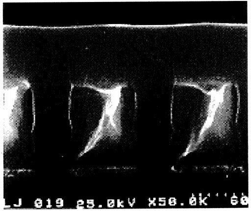
2. Gap Fill
When the gap between metal lines narrows to 0.25 µm with an aspect ratio of 4:1, most CVD deposition techniques struggle to fill the gaps without voids. High-Density Plasma CVD (HDP-CVD) is capable of filling such narrow gaps without creating voids (see figure below). The HDP-CVD process will be described subsequently.
3. Plasma Etching
Compared to wet etching, plasma etching offers advantages such as anisotropic etch profiles, automatic end-point detection, and lower chemical consumption, along with reasonable high etch rates, good selectivity, and uniformity.
4. Control of Etch Profiles
Before plasma etching became widespread in semiconductor manufacturing, most wafer fabs used wet chemical etching for pattern transfer. However, wet etching is an isotropic process (etching at the same rate in every direction). When feature sizes shrink below 3 µm, isotropic etching results in undercutting, limiting the application of wet etching.
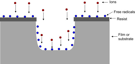
In plasma processes, ions continuously bombard the wafer surface. Whether through lattice damage mechanisms or sidewall passivation mechanisms, plasma etching can achieve anisotropic etch profiles. By reducing the pressure during the etching process, the mean free path of ions can be increased, thereby reducing ion collisions for better profile control.
5. Etch Rate and Selectivity
Ion bombardment in the plasma helps break the chemical bonds of surface atoms, exposing them to radicals generated by the plasma. This combination of physical and chemical treatment significantly enhances the chemical reaction rate of etching. The etch rate and selectivity are dictated by the process requirements. Since both ion bombardment and radicals play crucial roles in etching, and RF power can control the ion bombardment and radicals, RF power becomes a key parameter for controlling the etch rate. Increasing RF power can significantly enhance the etch rate, which will be discussed in further detail, also affecting the selectivity.
6. End-point Detection
Without plasma, the etch end-point must be determined by time or operator visual inspection. In plasma processes, as etching progresses through the surface material to begin etching the underlying (end-point) material, the chemical composition of the plasma changes due to the alteration in etch by-products, evident through a change in the emission color. By monitoring the change in emission color with optical sensors, the etch end-point can be automatically processed. In IC production, this is a highly valuable tool.**


