- English
- Español
- Português
- русский
- Français
- 日本語
- Deutsch
- tiếng Việt
- Italiano
- Nederlands
- ภาษาไทย
- Polski
- 한국어
- Svenska
- magyar
- Malay
- বাংলা ভাষার
- Dansk
- Suomi
- हिन्दी
- Pilipino
- Türkçe
- Gaeilge
- العربية
- Indonesia
- Norsk
- تمل
- český
- ελληνικά
- український
- Javanese
- فارسی
- தமிழ்
- తెలుగు
- नेपाली
- Burmese
- български
- ລາວ
- Latine
- Қазақша
- Euskal
- Azərbaycan
- Slovenský jazyk
- Македонски
- Lietuvos
- Eesti Keel
- Română
- Slovenski
- मराठी
- Srpski језик

Silicon Epitaxial Layers and Substrates in Semiconductor Manufacturing
2024-05-07
In the semiconductor manufacturing process, silicon epitaxial layers and substrates are two fundamental components that play crucial roles. The substrate, primarily made of single-crystal silicon, serves as the foundation for semiconductor chip manufacturing. It can directly enter the wafer fabrication flow to produce semiconductor devices or be further processed through epitaxial techniques to create an epitaxial wafer. As the foundational “base” of semiconductor structures, the substrate ensures the structural integrity, preventing any fractures or damage. Additionally, substrates possess distinctive electrical, optical, and mechanical properties critical to the performance of semiconductors.
If integrated circuits are likened to skyscrapers, then the substrate is undoubtedly the stable foundation. To ensure its supportive role, these materials must exhibit a high degree of uniformity in their crystal structure, akin to high-purity single-crystal silicon. The purity and perfection are fundamental to establishing a robust foundation. Only with a solid and reliable base can the upper structures be stable and flawless. Simply put, without a suitable substrate, it is impossible to construct stable and well-performing semiconductor devices.

Epitaxy refers to the process of precisely growing a new single-crystal layer on a meticulously cut and polished single-crystal substrate. This new layer may be of the same material as the substrate (homogeneous epitaxy) or different (heterogeneous epitaxy). Since the new crystal layer strictly follows the extension of the substrate’s crystal phase, it is known as an epitaxial layer, typically maintained at micrometer-level thickness. For instance, in silicon epitaxy, growth occurs on a specific crystallographic orientation of a silicon single-crystal substrate, forming a new crystal layer that is consistent in orientation but varies in electrical resistivity and thickness, and possesses a flawless lattice structure. The substrate that has undergone epitaxial growth is termed an epitaxial wafer, with the epitaxial layer being the core value around which device fabrication revolves.
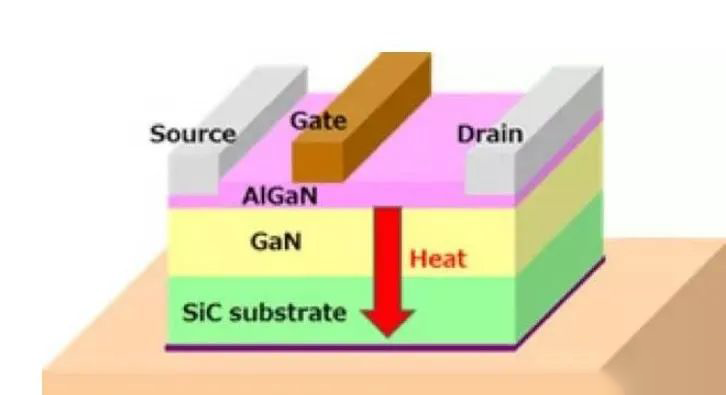
The value of an epitaxial wafer lies in its ingenious combination of materials. For example, by growing a thin layer of GaN epitaxy on a less expensive silicon wafer, it is possible to achieve the high-performance wide-bandgap characteristics of third-generation semiconductors at a relatively lower cost using first-generation semiconductor materials as the substrate. However, heterogeneous epitaxial structures also present challenges such as lattice mismatch, inconsistency in thermal coefficients, and poor thermal conductivity, akin to setting up scaffolding on a plastic base. Different materials expand and contract at different rates when temperatures change, and silicon’s thermal conductivity is not ideal.
Homogeneous epitaxy, which grows an epitaxial layer of the same material as the substrate, is significant for enhancing the stability and reliability of the product. Although the materials are the same, epitaxial processing significantly improves the purity and uniformity of the wafer surface compared to mechanically polished wafers. The epitaxial surface is smoother and cleaner, with significantly reduced micro-defects and impurities, more uniform electrical resistivity, and more precise control over surface particles, layer faults, and dislocations. Thus, epitaxy not only optimizes product performance but also ensures product stability and reliability.**
Semicorex offers high-quality substrates and epitaxial wafers. If you have any inquiries or need additional details, please don't hesitate to get in touch with us.
Contact phone # +86-13567891907
Email: sales@semicorex.com
Previous:Advantages of SiC in EV industry