- English
- Español
- Português
- русский
- Français
- 日本語
- Deutsch
- tiếng Việt
- Italiano
- Nederlands
- ภาษาไทย
- Polski
- 한국어
- Svenska
- magyar
- Malay
- বাংলা ভাষার
- Dansk
- Suomi
- हिन्दी
- Pilipino
- Türkçe
- Gaeilge
- العربية
- Indonesia
- Norsk
- تمل
- český
- ελληνικά
- український
- Javanese
- فارسی
- தமிழ்
- తెలుగు
- नेपाली
- Burmese
- български
- ລາວ
- Latine
- Қазақша
- Euskal
- Azərbaycan
- Slovenský jazyk
- Македонски
- Lietuvos
- Eesti Keel
- Română
- Slovenski
- मराठी
- Srpski језик
The Application Prospects of 12-Inch Silicon Carbide Substrates
2025-01-10
What Are the Material Characteristics and Technical Requirements of 12-Inch Silicon Carbide Substrates?
A. Basic Physical and Chemical Characteristics of Silicon Carbide
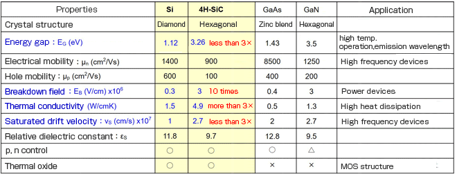
One of Silicon Carbide's most prominent features is its wide bandgap width, approximately 3.26 eV for 4H-SiC or 3.02 eV for 6H-SiC, significantly higher than silicon's 1.1 eV. This wide bandgap allows SiC to operate under extremely high electric field strengths and withstand significant heat without thermal breakdown or breakdown, making it the preferred material for electronic devices in high-voltage, high-temperature environments.

High Breakdown Electric Field: The high breakdown electric field of SiC (about 10 times that of silicon) enables it to work stably under high voltage, achieving high power density and efficiency in power electronic systems, especially in electric vehicles, power converters, and industrial power supplies.
High-Temperature Resistance: SiC's high thermal conductivity and ability to withstand high temperatures (up to 600°C or higher) make it an ideal choice for devices required to operate in extreme environments, particularly in the automotive and aerospace industries.
High-Frequency Performance: Although SiC's electron mobility is lower than silicon, it is still sufficient to support high-frequency applications. Therefore, SiC plays a crucial role in high-frequency fields such as wireless communication, radar, and high-frequency power amplifiers.
Radiation Resistance: SiC's strong radiation resistance is particularly evident in space devices and nuclear energy electronics, where it can withstand interference from external radiation without significant degradation of material performance.
B. Key Technical Indicators of 12-Inch Substrates
The advantages of 12-inch (300mm) silicon carbide substrates are not only reflected in the increase in size but also in their comprehensive technical requirements, which directly determine the manufacturing difficulty and the performance of the final devices.
Crystal Structure: SiC mainly has two common crystal structures—4H-SiC and 6H-SiC. 4H-SiC, with its higher electron mobility and excellent thermal conductivity, is more suitable for high-frequency and high-power applications, while 6H-SiC has a higher defect density and poorer electronic performance, typically used for low-power, low-frequency applications. For 12-inch substrates, choosing the appropriate crystal structure is crucial. 4H-SiC, with fewer crystal defects, is more suitable for high-frequency, high-power applications.
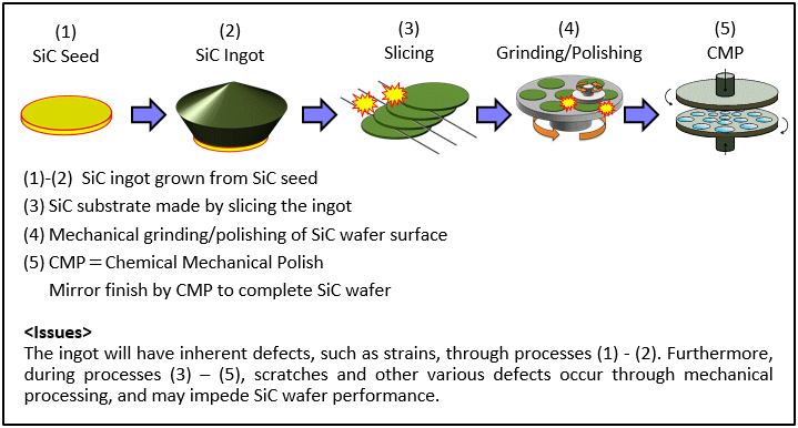
Substrate Surface Quality: The surface quality of the substrate has a direct impact on device performance. Surface smoothness, roughness, and defect density all need to be strictly controlled. A rough surface not only affects the crystalline quality of the device but can also lead to early device failure. Therefore, improving the substrate's surface smoothness through technologies such as Chemical Mechanical Polishing (CMP) is crucial.
Thickness and Uniformity Control: The increased size of 12-inch substrates means higher requirements for thickness uniformity and crystal quality. Inconsistent thickness can lead to uneven thermal stress, affecting the performance and reliability of the device. To ensure high-quality 12-inch substrates, precise growth and subsequent cutting and polishing processes must be employed to guarantee thickness consistency.
C. Size and Production Advantages of 12-Inch Substrates
As the semiconductor industry moves towards larger substrates, 12-inch silicon carbide substrates offer significant advantages in production efficiency and cost-effectiveness. Compared to traditional 6-inch and 8-inch substrates, 12-inch substrates can provide more chip cuts, greatly increasing the number of chips produced per production run, thereby significantly reducing the unit chip cost. In addition, the larger size of 12-inch substrates provides a better platform for the efficient production of integrated circuits, reducing repetitive production steps and improving overall production efficiency.

How Are 12-Inch Silicon Carbide Substrates Manufactured?
A. Crystal Growth Techniques
Sublimation Method (PVT):
The Sublimation Method (Physical Vapor Transport, PVT) is one of the most commonly used silicon carbide crystal growth techniques, especially suitable for the production of large-sized silicon carbide substrates. In this process, silicon carbide raw materials sublime at high temperatures, and the gaseous carbon and silicon recombine on the hot substrate to grow into crystals. The advantages of the sublimation method include high material purity and good crystal quality, suitable for the production of high-demand 12-inch substrates. However, this method also faces some challenges, such as slow growth rates and high requirements for strict control of temperature and atmosphere.
CVD Method (Chemical Vapor Deposition):
In the CVD process, gaseous precursors (such as SiCl₄ and C₆H₆) decompose and deposit onto the substrate to form a film at high temperatures. Compared to PVT, the CVD method can provide more uniform film growth and is suitable for the accumulation of thin film materials and surface functionalization. Although the CVD method has some difficulties in thickness control, it is still widely used to improve crystal quality and substrate uniformity.
B. Substrate Cutting and Polishing Techniques
Crystal Cutting:
Cutting 12-inch substrates from large-sized crystals is a complex technique. The crystal cutting process requires precise control of mechanical stress to ensure that the substrate does not crack or develop microcracks during cutting. To improve cutting accuracy, laser cutting technology is often used, or combined with ultrasonic and high-precision mechanical tools to enhance cutting quality.
Polishing and Surface Treatment:
Chemical Mechanical Polishing (CMP) is a key technology for improving substrate surface quality. This process removes micro-defects on the substrate surface through the synergistic action of mechanical friction and chemical reactions, ensuring smoothness and flatness. Surface treatment not only improves the substrate's glossiness but also reduces surface defects, thereby optimizing the performance of subsequent devices.

C. Substrate Defect Control and Quality Inspection
Defect Types:
Common defects in silicon carbide substrates include dislocations, lattice defects, and microcracks. These defects can directly affect the electrical performance and thermal stability of devices. Therefore, it is essential to strictly control the occurrence of these defects during substrate growth, cutting, and polishing. Dislocations and lattice defects usually originate from improper crystal growth or excessive cutting temperatures.
Quality Assessment:
To ensure substrate quality, technologies such as Scanning Electron Microscopy (SEM) and Atomic Force Microscopy (AFM) are commonly used for surface quality inspection. Additionally, electrical performance tests (such as conductivity and mobility) can further assess substrate quality.
In Which Fields Are 12-Inch Silicon Carbide Substrates Applied?
A. Power Electronics and Power Semiconductor Devices
12-inch silicon carbide substrates are widely used in power semiconductor devices, particularly in MOSFETs, IGBTs, and Schottky diodes. These devices are extensively applied in efficient power management, industrial power supplies, converters, and electric vehicles. The high voltage tolerance and low switching loss characteristics of SiC devices enable them to significantly improve power conversion efficiency, reduce energy loss, and promote the development of green energy technologies.
B. New Energy and Electric Vehicles
In electric vehicles, 12-inch silicon carbide substrates can enhance the efficiency of electric drive systems and improve battery charging speed and range. Due to the ability of silicon carbide materials to effectively handle high voltage and high-frequency signals, they are also indispensable in high-speed charging equipment at electric vehicle charging stations.
C. 5G Communications and High-Frequency Electronics
12-inch silicon carbide substrates, with their excellent high-frequency performance, are widely used in 5G base stations and high-frequency RF devices. They can significantly improve signal transmission efficiency and reduce signal loss, supporting the high-speed data transmission of 5G networks.
D. Energy Sector
Silicon carbide substrates also have important applications in renewable energy fields such as photovoltaic inverters and wind power generation. By improving energy conversion efficiency, SiC devices can reduce energy loss and enhance the stability and reliability of power grid equipment.

What Are the Challenges and Bottlenecks of 12-Inch Silicon Carbide Substrates?
A. Manufacturing Costs and Large-Scale Production
The production cost of 12-inch silicon carbide wafers remains high, mainly reflected in raw materials, equipment investment, and technology research and development. How to break through the technical challenges of large-scale production and reduce unit manufacturing costs is key to promoting the popularization of silicon carbide technology.
B. Substrate Defects and Quality Consistency
Although 12-inch substrates have production advantages, defects may still occur during their crystal growth, cutting, and polishing processes, leading to inconsistent substrate quality. How to reduce defect density and improve quality consistency through innovative technologies is a focus of future research.
C. Demand for Equipment and Technology Updates
The demand for high-precision cutting and polishing equipment is increasing. At the same time, precise quality inspection of substrates based on new detection technologies (such as atomic force microscopy, electron beam scanning, etc.) is key to improving production efficiency and product quality.
We at Semicorex provide a range of High-quality Wafers meticulously engineered to meet the demanding requirements of the semiconductor industry, if you have any inquiries or need additional details, please don't hesitate to get in touch with us.
Contact phone: +86-13567891907
Email: sales@semicorex.com


