- English
- Español
- Português
- русский
- Français
- 日本語
- Deutsch
- tiếng Việt
- Italiano
- Nederlands
- ภาษาไทย
- Polski
- 한국어
- Svenska
- magyar
- Malay
- বাংলা ভাষার
- Dansk
- Suomi
- हिन्दी
- Pilipino
- Türkçe
- Gaeilge
- العربية
- Indonesia
- Norsk
- تمل
- český
- ελληνικά
- український
- Javanese
- فارسی
- தமிழ்
- తెలుగు
- नेपाली
- Burmese
- български
- ລາວ
- Latine
- Қазақша
- Euskal
- Azərbaycan
- Slovenský jazyk
- Македонски
- Lietuvos
- Eesti Keel
- Română
- Slovenski
- मराठी
- Srpski језик
Wafer manufacturing
2025-01-10
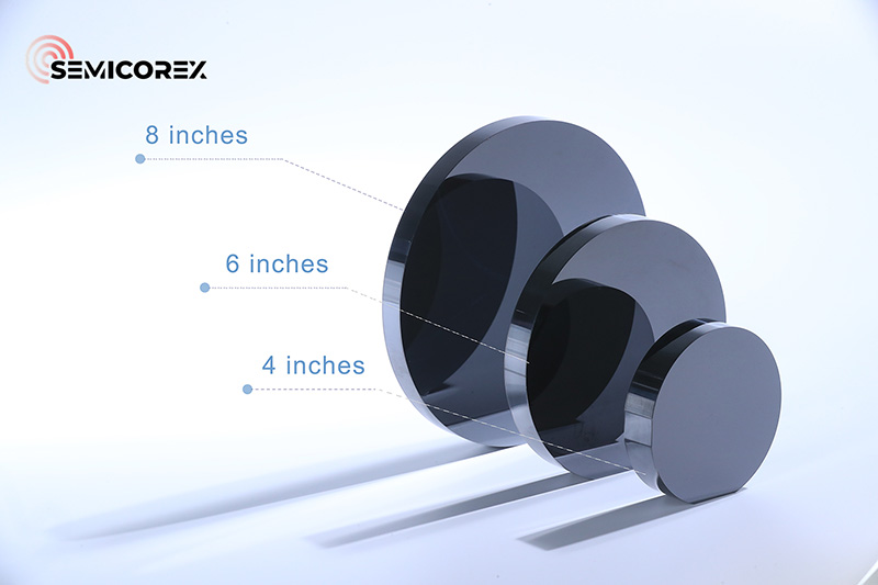
As technology advances, the demand for wafers continues to rise. Currently, the mainstream sizes of silicon wafers in the domestic market are 100mm, 150mm, and 200mm. Increasing the diameter of silicon wafers can reduce the manufacturing cost of each chip, leading to a growing demand for 300mm silicon wafers. However, larger diameters also impose stricter requirements on key parameters, such as wafer surface flatness, trace impurity control, internal defects, and oxygen content. Consequently, wafer manufacturing has become a primary focus of research in chip production.

Before delving into wafer manufacturing, it is essential to understand the underlying crystal structure.
The difference in the internal atomic organization of materials is a crucial factor in distinguishing between them. Crystalline materials, such as silicon and germanium, have atoms arranged in a fixed periodic structure, while non-crystalline materials, like plastics, lack this ordered arrangement. Silicon has emerged as the primary material for wafers due to its unique structure, favorable chemical properties, natural abundance, and other advantages.
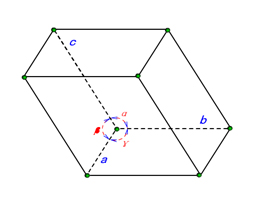
Crystalline materials possess two levels of atomic organization. The first level is the structure of individual atoms, forming a unit cell that is periodically repeated throughout the crystal. The second level refers to the overall arrangement of these unit cells, known as the lattice structure, where atoms occupy specific positions within the lattice. The number of atoms in the unit cell, their relative positions, and the binding energy between them determine the various properties of the material. Silicon crystal structure is categorized as a diamond structure, composed of two sets of face-centered cubic lattices offset along the diagonal by one-quarter of the diagonal length.

The characteristics of periodicity and symmetry in crystals necessitate a simpler method for describing the positions of atoms rather than using a universal three-dimensional rectangular coordinate system. To better describe the atomic distribution in a crystal based on its lattice periodicity, we select a unit cell according to three guiding principles. This unit cell effectively reflects the periodicity and symmetry of the crystal and serves as the smallest repeating unit. Once the atomic coordinates within the unit cell are determined, we can easily infer the relative positions of the particles throughout the entire crystal. By establishing a coordinate system based on the three edge vectors of the unit cell, we can simplify the process of describing the crystal structure significantly.
A crystal plane is defined as a flat surface formed by the arrangement of atoms, ions, or molecules within a crystal. Conversely, a crystal direction refers to a specific orientation of these atomic arrangements.
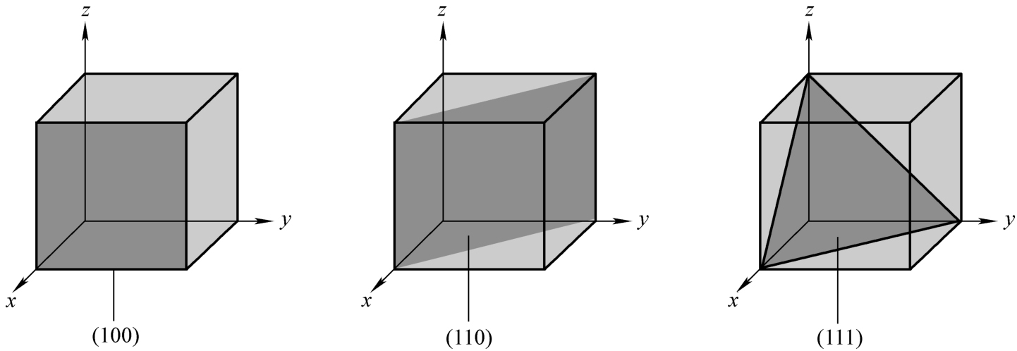
Crystal planes are represented using Miller indices. Typically, parentheses () denote crystal planes, square brackets [] indicate crystal directions, angle brackets <> signify families of crystal directions, and curly brackets {} represent families of crystal planes. In semiconductor manufacturing, the most commonly used crystal planes for silicon wafers are (100), (110), and (111). Each crystal plane possesses unique characteristics, making them suitable for different production processes.
For instance, (100) crystal planes are predominantly used in the manufacturing of MOS devices due to their favorable surface properties, which facilitate control over the threshold voltage. Additionally, wafers with (100) crystal planes are easier to handle during processing and have relatively flat surfaces, making them ideal for producing large-scale integrated circuits. In contrast, (111) crystal planes, which have a higher atomic density and lower growth costs, are often utilized in bipolar devices. These planes can be achieved by carefully managing the crystal direction during the growth process by selecting the appropriate direction of the seed crystal.
The (100) crystal plane is parallel to the Y-Z axis and intersects the X-axis at the point where the unit value is 1. The (110) crystal plane intersects both the X and Y axes, while the (111) crystal plane intersects all three axes: X, Y, and Z.

In a structural perspective, the (100) crystal plane forms a square shape, whereas the (111) crystal plane takes on a triangular shape. Due to the variations in structure among different crystal planes, the manner in which a wafer breaks also differs. Wafers oriented along <100> tend to break into square shapes or create breaks at right angles (90°), while those oriented along <111> break into triangular fragments.
Given the unique chemical, electrical, and physical properties associated with the internal structures of crystals, the specific crystal orientation of a wafer significantly impacts its overall performance. Consequently, it is crucial to maintain strict control over the crystal orientation during the preparation process.
Semicorex offers high-quality semiconductor wafers. If you have any inquiries or need additional details, please don't hesitate to get in touch with us.
Contact phone # +86-13567891907
Email: sales@semicorex.com


