- English
- Español
- Português
- русский
- Français
- 日本語
- Deutsch
- tiếng Việt
- Italiano
- Nederlands
- ภาษาไทย
- Polski
- 한국어
- Svenska
- magyar
- Malay
- বাংলা ভাষার
- Dansk
- Suomi
- हिन्दी
- Pilipino
- Türkçe
- Gaeilge
- العربية
- Indonesia
- Norsk
- تمل
- český
- ελληνικά
- український
- Javanese
- فارسی
- தமிழ்
- తెలుగు
- नेपाली
- Burmese
- български
- ລາວ
- Latine
- Қазақша
- Euskal
- Azərbaycan
- Slovenský jazyk
- Македонски
- Lietuvos
- Eesti Keel
- Română
- Slovenski
- मराठी
- Srpski језик
What Are the Applications of SiC and TaC Coatings in the Semiconductor Field?
2024-11-18
How is the Semiconductor Sector Broadly Defined and What are Its Main Components?
The semiconductor sector broadly refers to the use of semiconductor materials’ properties to produce semiconductor integrated circuits (ICs), semiconductor displays (LCD/OLED panels), semiconductor lighting (LED), and semiconductor energy products (photovoltaics) through related semiconductor manufacturing processes. Integrated circuits account for up to 80% of this sector, so, narrowly speaking, the semiconductor industry often refers specifically to the IC industry.
In essence, semiconductor manufacturing involves creating circuit structures on a “substrate” and connecting this circuit to external power and control systems to achieve various functionalities. Substrates, a term used in the industry, can be made of semiconductor materials like Si or SiC, or non-semiconductor materials like sapphire or glass. Except for the LED and panel industries, silicon wafers are the most commonly used substrates. Epitaxy refers to the process of growing a new thin-film material on the substrate, with common materials being Si, SiC, GaN, GaAs, etc. Epitaxy provides significant flexibility for device designers to optimize device performance by controlling factors like the doping thickness, concentration, and profile of the epitaxial layer, independent of the substrate. This control is achieved through doping during the epitaxial growth process.
What Comprises the Front-end Process in Semiconductor Manufacturing?
The front-end process is the most technically complex and capital-intensive part of semiconductor manufacturing, requiring the repetition of the same procedures multiple times, hence termed a “cyclic process.” It primarily includes cleaning, oxidation, photolithography, etching, ion implantation, diffusion, annealing, thin-film deposition, and polishing.
How do Coatings Protect Semiconductor Manufacturing Equipment?
Semiconductor manufacturing equipment operates in high-temperature, highly corrosive environments and demands extremely high cleanliness. Thus, protecting the internal components of the equipment is a crucial challenge. Coating technology enhances and protects the base materials by forming a thin covering layer on their surfaces. This adaptation allows the base materials to withstand more extreme and complex production environments, improving their high-temperature stability, corrosion resistance, oxidation resistance, and extending their lifespan.
Why is SiC Coating Significant in the Silicon Substrate Manufacturing Domain?
In silicon crystal growth furnaces, high-temperature silicon vapor around 1500°C can significantly corrode graphite or carbon-carbon material components. Applying a high-purity SiC coating on these components can effectively block silicon vapor and extend the components’ service life.
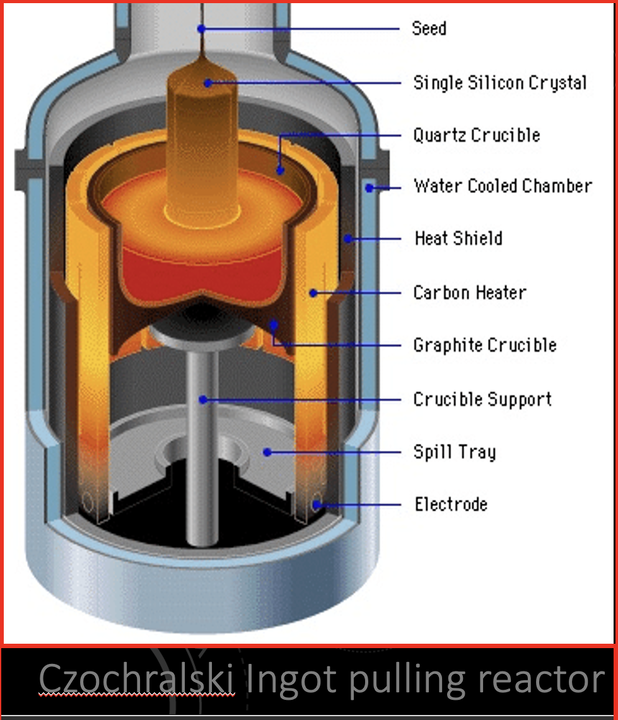
The production process of semiconductor silicon wafers is complex, involving numerous steps, with crystal growth, silicon wafer forming, and epitaxial growth being the primary stages. Crystal growth is the core process in silicon wafer production. During the single-crystal preparation phase, crucial technical parameters such as wafer diameter, crystal orientation, doping conductivity type, resistivity range and distribution, carbon and oxygen concentration, and lattice defects are determined. Single-crystal silicon is typically prepared using either the Czochralski (CZ) method or the Float Zone (FZ) method. The CZ method is the most commonly used, accounting for about 85% of silicon single crystals. 12-inch silicon wafers can only be produced using the CZ method. This method involves placing high-purity polysilicon material in a quartz crucible, melting it under the protection of high-purity inert gas, and then inserting a single-crystal silicon seed into the melt. As the seed is pulled up, the crystal grows into a monocrystalline silicon rod.

How is TaC Coating Evolving with PVT Methods?
The inherent characteristics of SiC (lack of a Si:C=1:1 liquid phase at atmospheric pressure) make single-crystal growth challenging. Currently, mainstream methods include Physical Vapor Transport (PVT), High-Temperature Chemical Vapor Deposition (HT-CVD), and Liquid Phase Epitaxy (LPE). Among these, PVT is the most widely adopted due to its lower equipment requirements, simpler process, strong controllability, and established industrial applications.
PVT method allows control over axial and radial temperature fields by adjusting the thermal insulation conditions outside the graphite crucible. SiC powder is placed at the hotter bottom of the graphite crucible, while the SiC seed crystal is fixed at the cooler top. The distance between the powder and the seed is typically controlled to several tens of millimeters to avoid contact between the growing SiC crystal and the powder. Using different heating methods (induction or resistance heating), the SiC powder is heated to 2200-2500°C, causing the original powder to sublimate and decompose into gaseous components such as Si, Si2C, and SiC2. These gases are transported to the seed crystal end by convection, where SiC crystalizes, achieving single-crystal growth. The typical growth rate is 0.2-0.4mm/h, requiring 7-14 days to grow a 20-30mm crystal ingot.
The presence of carbon inclusions in PVT-grown SiC crystals is a significant defect source, contributing to microtubes and polymorphic defects, which degrade the quality of SiC crystals and limit the performance of SiC-based devices. Generally, the graphitization of SiC powder and a carbon-rich growth front are recognized sources of carbon inclusions: 1) During SiC powder decomposition, Si vapor accumulates in the gas phase while C concentrates in the solid phase, leading to severe carbonization of the powder late in growth. Once carbon particles in the powder overcome gravity and diffuse into the SiC ingot, carbon inclusions form. 2) Under Si-rich conditions, excess Si vapor reacts with the graphite crucible wall, forming a thin SiC layer that can easily decompose into carbon particles and Si-containing components.
Two approaches can address these issues: 1) Filter carbon particles from heavily carbonized SiC powder late in growth. 2) Prevent Si vapor from corroding the graphite crucible wall. Many carbides, such as TaC, can operate stably above 2000°C and resist chemical corrosion by acids, alkalis, NH3, H2, and Si vapor. With increasing quality demands for SiC wafers, the application of TaC coatings in SiC crystal growth technology is being explored industrially. Studies show that SiC crystals prepared using TaC-coated graphite components in PVT growth furnaces are purer, with significantly reduced defect densities, substantially enhancing crystal quality.
a) Porous TaC or TaC-coated porous graphite: Filters carbon particles, prevents diffusion into the crystal, and ensures uniform airflow.
b) TaC-coated rings: Isolate Si vapor from the graphite crucible wall, preventing crucible wall corrosion by Si vapor.
c) TaC-coated flow guides: Isolate Si vapor from the graphite crucible wall while directing airflow towards the seed crystal.
d) TaC-coated seed crystal holders: Isolate Si vapor from the crucible’s top cover to prevent top cover corrosion by Si vapor.
How does CVD SiC Coating Benefit in GaN Substrate Manufacturing?
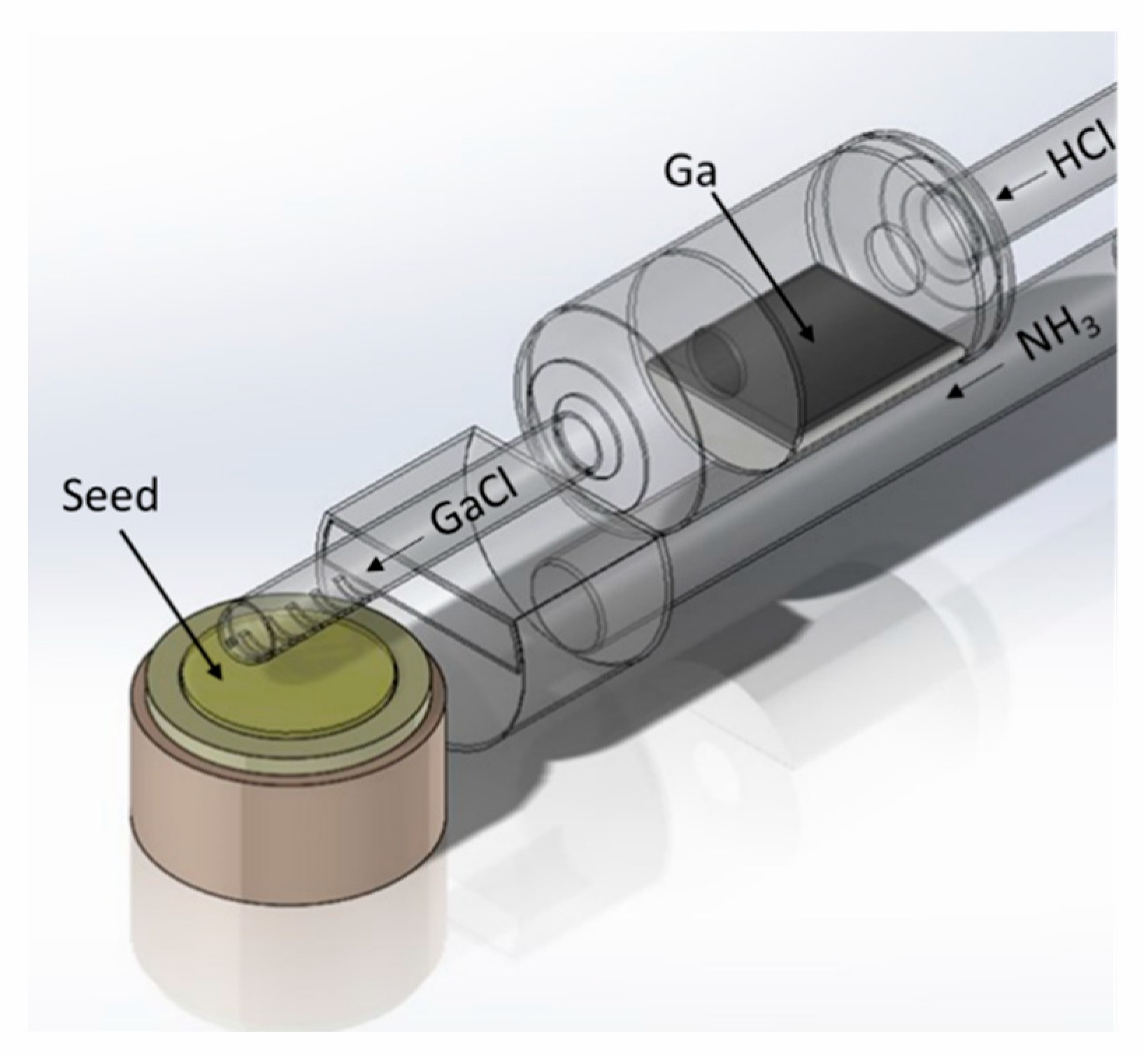
Currently, the commercial production of GaN substrates begins with the creation of a buffer layer (or mask layer) on a sapphire substrate. Hydrogen Vapor Phase Epitaxy (HVPE) is then used to rapidly grow a GaN film on this buffer layer, followed by separation and polishing to obtain a free-standing GaN substrate. How does HVPE operate within atmospheric pressure quartz reactors, given its requirement for both low and high-temperature chemical reactions?
In the low-temperature zone (800-900°C), gaseous HCl reacts with metallic Ga to produce gaseous GaCl.
In the high-temperature zone (1000-1100°C), gaseous GaCl reacts with gaseous NH3 to form a GaN single-crystal film.
What are the structural components of HVPE equipment, and how are they protected from corrosion? HVPE equipment can be either horizontal or vertical, consisting of components such as the gallium boat, furnace body, reactor, gas configuration system, and exhaust system. Graphite trays and rods, which come into contact with NH3, are susceptible to corrosion and can be protected with a SiC coating to prevent damage.

What is the Importance of CVD Technology over GaN Epitaxy Manufacturing?
In the field of semiconductor devices, why is it necessary to construct epitaxial layers on certain wafer substrates? A typical example includes blue-green LEDs, which require GaN epitaxial layers on sapphire substrates. MOCVD equipment is vital in the GaN epitaxy production process, with the leading suppliers being AMEC, Aixtron, and Veeco in China.
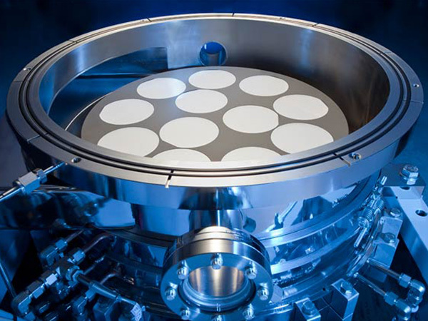
Why can’t substrates be placed directly on metal or simple bases during epitaxial deposition in MOCVD systems? Factors such as gas flow direction (horizontal, vertical), temperature, pressure, substrate fixation, and contamination from debris must be considered. Therefore, a susceptor with pockets is used to hold the substrates, and epitaxial deposition is performed using CVD technology on substrates placed in these pockets. The susceptor is a graphite base with a SiC coating.
What is the core chemical reaction in GaN epitaxy, and why is the quality of the SiC coating crucial? The core reaction is NH3 + TMGa → GaN + byproducts (at approximately 1050-1100°C). However, NH3 thermally decomposes at high temperatures, releasing atomic hydrogen, which reacts strongly with the carbon in graphite. Since NH3/H2 does not react with SiC at 1100°C, the complete encapsulation by and quality of the SiC coating are critical to the process.
In the Field of SiC Epitaxy Manufacturing, How are Coatings Applied within Mainstream Types of Reaction Chambers?
SiC is a typical polytypic material with over 200 different crystal structures, among which 3C-SiC, 4H-SiC, and 6H-SiC are the most common. The 4H-SiC is the crystal structure predominantly used in mainstream devices. A significant factor influencing the crystal structure is the reaction temperature. Temperatures below a specific threshold tend to produce other crystal forms. The optimal reaction temperature is between 1550 and 1650°C; temperatures below 1550°C are more likely to yield 3C-SiC and other structures. However, 3C-SiC is commonly used in SiC coatings, and a reaction temperature of around 1600°C is close to the limit of 3C-SiC. Although the current application of TaC coatings is limited by cost issues, in the long term, TaC coatings are expected to gradually replace SiC coatings in SiC epitaxial equipment.
Currently, there are three main types of CVD systems for SiC epitaxy: planetary hot-wall, horizontal hot-wall, and vertical hot-wall. The planetary hot-wall CVD system is characterized by its ability to grow multiple wafers in a single batch, resulting in high production efficiency. The horizontal hot-wall CVD system typically involves a single-wafer, large-size growth system driven by gas float rotation, which facilitates excellent intra-wafer specifications. The vertical hot-wall CVD system mainly features high-speed rotation assisted by an external mechanical base. It effectively reduces the thickness of the boundary layer by maintaining lower reaction chamber pressure, thus enhancing the epitaxial growth rate. Additionally, its chamber design lacks a top wall that could lead to SiC particle deposition, minimizing the risk of particle fall-off and providing an inherent advantage in defect control.

For High-Temperature Thermal Processing, What is the Applications of CVD SiC in Tube Furnace Equipment?
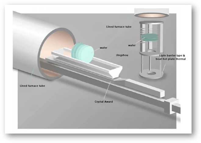
Tube furnace equipment is widely used in processes such as oxidation, diffusion, thin-film growth, annealing, and alloying in the semiconductor industry. There are two main types: horizontal and vertical. Currently, the IC industry primarily utilizes vertical tube furnaces. Depending on process pressure and application, tube furnace equipment can be categorized into atmospheric pressure furnaces and low-pressure furnaces. Atmospheric pressure furnaces are mainly used for thermal diffusion doping, thin-film oxidation, and high-temperature annealing, while low-pressure furnaces are designed for the growth of various types of thin films (such as LPCVD and ALD). The structures of various tube furnace equipment are similar, and they can be flexibly configured to perform diffusion, oxidation, annealing, LPCVD, and ALD functions as needed. High-purity sintered SiC tubes, SiC wafer boats, and SiC lining walls are essential components inside the reaction chamber of tube furnace equipment. Depending on customer requirements, an additional SiC coating layer can be applied to the surface of sintered SiC ceramics to enhance performance.

In the Field of Photovoltaic Granular Silicon Manufacturing, Why is SiC Coating Playing a Pivotal Role?
Polysilicon, derived from metallurgical-grade silicon (or industrial silicon), is a non-metallic material purified through a series of physical and chemical reactions to achieve a silicon content exceeding 99.9999% (6N). In the photovoltaic field, polysilicon is processed into wafers, cells, and modules, which are ultimately used in photovoltaic power generation systems, making polysilicon a crucial upstream component of the photovoltaic industry chain. Currently, there are two technological routes for polysilicon production: the modified Siemens process (yielding rod-like silicon) and the silane fluidized bed process (yielding granular silicon). In the modified Siemens process, high-purity SiHCl3 is reduced by high-purity hydrogen on a high-purity silicon core at around 1150°C, resulting in polysilicon deposition on the silicon core. The silane fluidized bed process typically uses SiH4 as the silicon source gas and H2 as the carrier gas, with the addition of SiCl4 to thermally decompose SiH4 in a fluidized bed reactor at 600-800°C to produce granular polysilicon. The modified Siemens process remains the mainstream polysilicon production route due to its relatively mature production technology. However, as companies like GCL-Poly and Tianhong Reike continue to advance granular silicon technology, the silane fluidized bed process may gain market share due to its lower cost and reduced carbon footprint.
Product purity control has historically been a weak point of the fluidized bed process, which is a primary reason why it has not surpassed the Siemens process despite its significant cost advantages. The lining serves as the main structure and reaction vessel of the silane fluidized bed process, protecting the metal shell of the reactor from erosion and wear by high-temperature gases and materials while insulating and maintaining the material’s temperature. Due to the harsh working conditions and direct contact with granular silicon, the lining material must exhibit high purity, wear resistance, corrosion resistance, and high strength. Common materials include graphite with a SiC coating. However, in actual use, there are occurrences of coating peeling/cracking that lead to excessive carbon content in granular silicon, resulting in a short lifespan for graphite linings and the need for regular replacement, classifying them as consumables. The technical challenges related to the SiC-coated fluidized bed lining materials and their high costs hinder the market adoption of the silane fluidized bed process and must be addressed for broader application.
In Which Applications is Pyrolytic Graphite Coating Utilized?
Pyrolytic graphite is a novel carbon material, consisting of high-purity hydrocarbons chemically vapor-deposited at furnace pressures between 1800°C and 2000°C, resulting in highly crystallographically oriented pyrolytic carbon. It features high density (2.20 g/cm³), high purity, and anisotropic thermal, electrical, magnetic, and mechanical properties. It can maintain a vacuum of 10mmHg even at approximately 1800°C, finding broad application potential in fields such as aerospace, semiconductors, photovoltaics, and analytical instruments.
In red-yellow LED epitaxy and certain special scenarios, the MOCVD ceiling does not require SiC coating protection and instead uses a pyrolytic graphite coating solution.
Crucibles for electron beam evaporation aluminum require high density, high-temperature resistance, good thermal shock resistance, high thermal conductivity, low thermal expansion coefficient, and resistance to corrosion by acids, alkalis, salts, and organic reagents. Since the pyrolytic graphite coating shares the same material as the graphite crucible, it can effectively withstand high-low temperature cycling, extending the service life of the graphite crucible.**


