- English
- Español
- Português
- русский
- Français
- 日本語
- Deutsch
- tiếng Việt
- Italiano
- Nederlands
- ภาษาไทย
- Polski
- 한국어
- Svenska
- magyar
- Malay
- বাংলা ভাষার
- Dansk
- Suomi
- हिन्दी
- Pilipino
- Türkçe
- Gaeilge
- العربية
- Indonesia
- Norsk
- تمل
- český
- ελληνικά
- український
- Javanese
- فارسی
- தமிழ்
- తెలుగు
- नेपाली
- Burmese
- български
- ລາວ
- Latine
- Қазақша
- Euskal
- Azərbaycan
- Slovenský jazyk
- Македонски
- Lietuvos
- Eesti Keel
- Română
- Slovenski
- मराठी
- Srpski језик
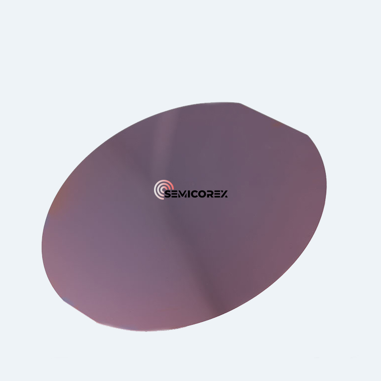
Surface Polishing of Silicon Wafers
Silicon wafer surface polishing is a crucial process in semiconductor manufacturing. Its primary goal is to achieve extremely high standards of surface flatness and roughness by removing micro-defects, layers of stress damage, and contamination from impurities such as metal ions. This ensures that the silicon wafers meet the preparation requirements for microelectronic devices, including integrated circuits (ICs).
To guarantee polishing accuracy, the silicon wafer polishing process can be organized into two, three, or even four distinct steps. Each step employs different processing conditions, including pressure, polishing liquid composition, particle size, concentration, pH value, polishing cloth material, structure, hardness, temperature, and processing volume.

The general stages of silicon wafer polishing are as follows:
1. **Rough Polishing**: This stage aims to remove the mechanical stress damage layer left on the surface from prior processing, achieving the required geometric dimensional accuracy. The processing volume for rough polishing typically exceeds 15–20μm.
2. **Fine Polishing**: In this stage, the local flatness and roughness of the silicon wafer surface are further minimized to ensure high surface quality. The processing volume for fine polishing is around 5–8μm.
3. **"Defogging" Fine Polishing**: This step focuses on eliminating tiny surface defects and improving the nano-morphology characteristics of the wafer. The amount of material removed during this process is about 1μm.
4. **Final Polishing**: For IC chip processes with extremely stringent linewidth requirements (such as chips smaller than 0.13μm or 28nm), a final polishing step is essential after fine polishing and "defogging" fine polishing. This ensures that the silicon wafer achieves exceptional machining accuracy and nanoscale surface characteristics.
It is important to note that the chemical mechanical polishing (CMP) of the silicon wafer surface is distinct from the CMP technology used for flattening the wafer surface in IC preparation. While both methods involve a combination of chemical and mechanical polishing, their conditions, purposes, and applications differ significantly.
Semicorex offers high-quality wafers. If you have any inquiries or need additional details, please don't hesitate to get in touch with us.
Contact phone # +86-13567891907
Email: sales@semicorex.com


