
- English
- Español
- Português
- русский
- Français
- 日本語
- Deutsch
- tiếng Việt
- Italiano
- Nederlands
- ภาษาไทย
- Polski
- 한국어
- Svenska
- magyar
- Malay
- বাংলা ভাষার
- Dansk
- Suomi
- हिन्दी
- Pilipino
- Türkçe
- Gaeilge
- العربية
- Indonesia
- Norsk
- تمل
- český
- ελληνικά
- український
- Javanese
- فارسی
- தமிழ்
- తెలుగు
- नेपाली
- Burmese
- български
- ລາວ
- Latine
- Қазақша
- Euskal
- Azərbaycan
- Slovenský jazyk
- Македонски
- Lietuvos
- Eesti Keel
- Română
- Slovenski
- मराठी
- Srpski језик

SiC Single Crystal Substrate Processing
Silicon Carbide (SiC) single crystals are primarily produced using the sublimation method. After removing the crystal from the crucible, several intricate processing steps are required to create usable wafers. The first step is to determine the crystal orientation of the SiC boule. Following this, the boule undergoes outer diameter grinding to achieve a cylindrical shape. For n-type SiC wafers, which are commonly used in power devices, both the upper and lower surfaces of the cylindrical crystal are typically machined to create a plane at a 4° angle relative to the {0001} face.
Next, the processing continues with directional edge or notch cutting to specify the crystal orientation of the wafer surface. In the production of large-diameter SiC wafers, directional notching is a common technique. The cylindrical SiC single crystal is then sliced into thin sheets, primarily using multi-wire cutting techniques. This process involves placing abrasives between the cutting wire and the SiC crystal while applying pressure to facilitate the cutting motion.

Fig. 1 Overview of SiC wafer processing technology
(a) Removing SiC ingot from crucible; (b) Cylindrical grinding; (c) Directional edge or notch cutting; (d) Multi-wire cutting; (e) Grinding and polishing
After slicing, the SiC wafers often show inconsistencies in thickness and surface irregularities, necessitating further flattening treatment. This begins with grinding to eliminate micron-level surface unevenness. During this phase, the abrasive action may introduce fine scratches and surface imperfections. Thus, the subsequent polishing step is crucial for attaining a mirror-like finish. Unlike grinding, polishing utilizes finer abrasives and requires meticulous care to prevent scratches or internal damage, ensuring a high degree of surface smoothness.
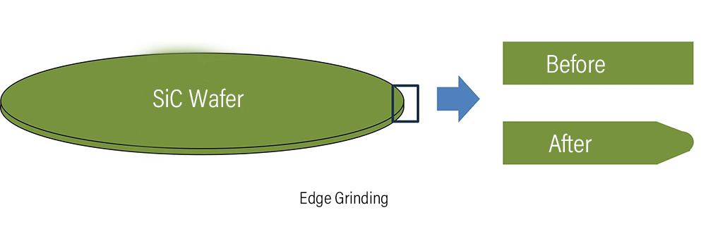
Through these procedures, SiC wafers evolve from rough processing to precision machining, ultimately resulting in a flat, mirror-like surface suitable for high-performance devices. However, addressing the sharp edges that often form around the perimeter of polished wafers is essential. These sharp edges are susceptible to breaking upon contact with other objects. To mitigate this fragility, edge grinding of the wafer perimeter is necessary. Industry standards have been established to ensure the reliability and safety of wafers during subsequent use.
SiC's exceptional hardness makes it an ideal abrasive material in various machining applications. However, this also presents challenges in processing SiC boules into wafers, as it is a time-consuming and complex process that is continuously being optimized. One promising innovation to improve traditional slicing methods is laser cutting technology. In this technique, a laser beam is directed from the top of the cylindrical SiC crystal, focusing at the desired cutting depth to create a modified zone within the crystal. By scanning the entire surface, this modified zone gradually expands into a plane, allowing for the separation of thin sheets. Compared to conventional multi-wire cutting, which often incurs significant kerf loss and may introduce surface irregularities, laser slicing significantly reduces kerf loss and processing time, positioning it as a promising method for future developments.
Another innovative slicing technology is the application of electrical discharge cutting, which generates discharges between a metal wire and the SiC crystal. This method boasts advantages in reducing kerf loss while further enhancing processing efficiency.
A distinctive approach to SiC wafer production involves adhering a thin film of SiC single crystal to a heterogeneous substrate, thereby fabricating SiC wafers. This bonding and detachment process begins with the injection of hydrogen ions into the SiC single crystal to a predetermined depth. The SiC crystal, now equipped with an ion-implanted layer, is layered onto a smooth supporting substrate, such as polycrystalline SiC. By applying pressure and heat, the SiC single crystal layer is transferred onto the supporting substrate, completing the detachment. The transferred SiC layer undergoes surface flattening treatment and can be reused in the bonding process. Although the cost of the supporting substrate is lower than that of SiC single crystals, technical challenges remain. Nevertheless, research and development in this area continue to advance actively, aiming to lower the overall manufacturing costs of SiC wafers.
In summary, the processing of SiC single crystal substrates involves multiple stages, from grinding and slicing to polishing and edge treatment. Innovations such as laser cutting and electrical discharge machining are improving efficiency and reducing material waste, while new methods of substrate bonding offer alternative pathways to cost-effective wafer production. As the industry continues to strive for improved techniques and standards, the ultimate goal remains the production of high-quality SiC wafers that meet the demands of advanced electronic devices.
Previous:Introducing Silicon Material


