
- English
- Español
- Português
- русский
- Français
- 日本語
- Deutsch
- tiếng Việt
- Italiano
- Nederlands
- ภาษาไทย
- Polski
- 한국어
- Svenska
- magyar
- Malay
- বাংলা ভাষার
- Dansk
- Suomi
- हिन्दी
- Pilipino
- Türkçe
- Gaeilge
- العربية
- Indonesia
- Norsk
- تمل
- český
- ελληνικά
- український
- Javanese
- فارسی
- தமிழ்
- తెలుగు
- नेपाली
- Burmese
- български
- ລາວ
- Latine
- Қазақша
- Euskal
- Azərbaycan
- Slovenský jazyk
- Македонски
- Lietuvos
- Eesti Keel
- Română
- Slovenski
- मराठी
- Srpski језик

Chip Manufacturing: Thin Film Processes
2024-10-07
What is the Basic Introduction to Thin Film Processes?
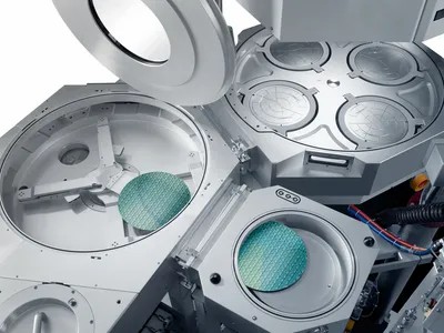
The semiconductor thin film deposition process is an essential component of modern microelectronics technology. It involves constructing complex integrated circuits by depositing one or more thin layers of material on a semiconductor substrate. These thin films can be metals, insulators, or semiconductor materials, each playing a different role in various layers of the chip, such as conduction, insulation, and protection. The quality of these thin films directly impacts the performance, reliability, and cost of the chip. Therefore, the development of thin film deposition technology is of significant importance to the semiconductor industry.
How are Thin Film Processes Classified?
Currently, mainstream thin film deposition equipment and techniques include Physical Vapor Deposition (PVD), Chemical Vapor Deposition (CVD), and Atomic Layer Deposition (ALD). These three techniques differ markedly in their deposition principles, materials, applicable film layers, and processes.
1. Physical Vapor Deposition (PVD)
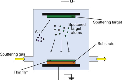
Physical Vapor Deposition (PVD) is a purely physical process where materials are vaporized through evaporation or sputtering and then condensed on the substrate to form a thin film.
Vacuum Evaporation: Materials are heated to vaporization under high vacuum conditions and deposited onto the substrate.
Sputtering: Gas ions generated by gas discharge bombard the target material at high speed, dislodging atoms that form a film on the substrate.
Ion Plating: Combines the advantages of vacuum evaporation and sputtering, where the vaporized material is partially ionized in the discharge space and attracted to the substrate to form a film.
Characteristics: PVD involves only physical changes without chemical reactions.
2. Chemical Vapor Deposition (CVD)
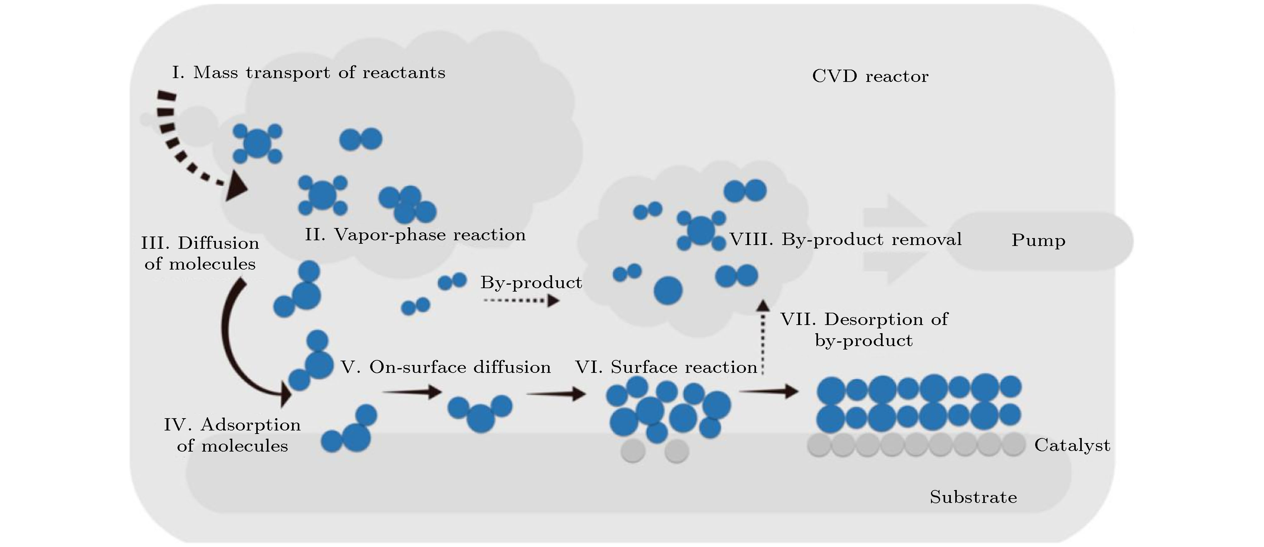
Chemical Vapor Deposition (CVD) is a technique that involves gas-phase chemical reactions to form solid thin films on the substrate.
Conventional CVD: Suitable for depositing various dielectric and semiconductor films.
Plasma-Enhanced CVD (PECVD): Uses plasma to enhance reaction activity, suitable for low-temperature deposition.
High-Density Plasma CVD (HDPCVD): Allows simultaneous deposition and etching, offering excellent high aspect ratio gap-filling capabilities.
Sub-Atmospheric CVD (SACVD): Achieves excellent hole-filling capabilities under high-pressure conditions by using highly reactive oxygen radicals formed at high temperatures.
Metal-Organic CVD (MOCVD): Suitable for semiconductor materials like GaN.
Characteristics: CVD involves gas-phase reactants such as silane, phosphine, borane, ammonia, and oxygen, producing solid films like nitrides, oxides, oxynitrides, carbides, and polysilicon under high-temperature, high-pressure, or plasma conditions.
3. Atomic Layer Deposition (ALD)
Atomic Layer Deposition (ALD) is a specialized CVD technique that involves alternating pulsed introductions of two or more reactants, achieving precise single-atomic-layer deposition.
Thermal ALD (TALD): Uses thermal energy for precursor adsorption and subsequent chemical reactions on the substrate.
Plasma-Enhanced ALD (PEALD): Uses plasma to enhance reaction activity, allowing faster deposition rates at lower temperatures.
Characteristics: ALD offers precise film thickness control, excellent uniformity, and consistency, making it highly suitable for film growth in deep trench structures.
How are Various Thin Film Processes Applied in Chips?
Metal Layers: PVD is primarily used for depositing ultra-pure metal and transition metal nitride films, such as aluminum pads, metal hard masks, copper barrier layers, and copper seed layers.
Al pad: Bonding pads for PCBs.
Metal Hard Mask: Commonly TiN, used in photolithography.
Cu Barrier Layer: Often TaN, prevents Cu diffusion.
Cu Seed Layer: Pure Cu or Cu alloy, used as a seed layer for subsequent electroplating.
Dielectric Layers: CVD is mainly used for depositing various insulating materials like nitrides, oxides, oxynitrides, carbides, and polysilicon, which isolate different circuit components and reduce interference.
Gate Oxide Layer: Isolates the gate and channel.
Interlayer Dielectric: Isolates different metal layers.
Barrier Layers: PVD is used to prevent metal diffusion and protect devices from contamination.
Cu Barrier Layer: Prevents copper diffusion, ensuring device performance.
Hard Masks: PVD is used in photolithography to help define device structures.
Metal Hard Mask: Commonly TiN, used to define patterns.
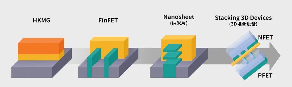
Self-Aligned Double Patterning (SADP): ALD uses spacer layers for finer patterning, suitable for manufacturing Fin structures in FinFETs.
FinFET: Uses spacer layers to create hard masks at the edges of core patterns, achieving spatial frequency multiplication.
High-K Metal Gate (HKMG): ALD is used to deposit high dielectric constant materials and metal gates, improving transistor performance, especially in 28nm and below processes.
High-K Dielectric Layer: HfO2 is the most common choice, with ALD being the preferred method of preparation.
Metal Gate: Developed due to the incompatibility of Hf elements with polysilicon gates.
Other Applications: ALD is also widely used in copper interconnect diffusion barrier layers and other technologies.
Copper Interconnect Diffusion Barrier Layer: Prevents copper diffusion, protecting device performance.
From the above introduction, we can observe that PVD, CVD, and ALD have unique characteristics and advantages, playing irreplaceable roles in semiconductor manufacturing. PVD is mainly used for metal film deposition, CVD is suitable for various dielectric and semiconductor film depositions, while ALD excels in advanced processes with its superior thickness control and step coverage capabilities. The continuous development and refinement of these technologies provide a solid foundation for the progress of the semiconductor industry.**
We at Semicorex specialize in CVD SiC/TaC coating components applied in semiconductor manufacturing, if you have any inquiries or need additional details, please don't hesitate to get in touch with us.
Contact phone: +86-13567891907
Email: sales@semicorex.com


