- English
- Español
- Português
- русский
- Français
- 日本語
- Deutsch
- tiếng Việt
- Italiano
- Nederlands
- ภาษาไทย
- Polski
- 한국어
- Svenska
- magyar
- Malay
- বাংলা ভাষার
- Dansk
- Suomi
- हिन्दी
- Pilipino
- Türkçe
- Gaeilge
- العربية
- Indonesia
- Norsk
- تمل
- český
- ελληνικά
- український
- Javanese
- فارسی
- தமிழ்
- తెలుగు
- नेपाली
- Burmese
- български
- ລາວ
- Latine
- Қазақша
- Euskal
- Azərbaycan
- Slovenský jazyk
- Македонски
- Lietuvos
- Eesti Keel
- Română
- Slovenski
- मराठी
- Srpski језик

Understanding the Etching Differences Between Silicon and Silicon Carbide Wafers
2024-09-05
In dry etching processes, particularly Reactive Ion Etching (RIE), the characteristics of the material being etched play a significant role in determining the etching rate and the final morphology of the etched structures. This is especially important when comparing the etching behaviors of silicon wafers and silicon carbide (SiC) wafers. While both are common materials in semiconductor manufacturing, their vastly different physical and chemical properties lead to contrasting etching outcomes.
Material Properties Comparison: Silicon vs. Silicon Carbide
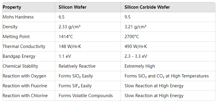
From the table, it's clear that SiC is much harder than silicon, with a Mohs hardness of 9.5, approaching that of diamond (Mohs hardness 10). Additionally, SiC exhibits far greater chemical inertness, meaning it requires highly specific conditions to undergo chemical reactions.
Etching Process: Silicon vs. Silicon Carbide
RIE etching involves both physical bombardment and chemical reactions. For materials like silicon, which are less hard and more chemically reactive, the process works efficiently. Silicon’s chemical reactivity allows for easier etching when exposed to reactive gases like fluorine or chlorine, and the physical bombardment by ions can easily disrupt the weaker bonds in the silicon lattice.
In contrast, SiC presents significant challenges in both the physical and chemical aspects of the etching process. The physical bombardment of SiC has less impact due to its higher hardness, and the Si-C covalent bonds have much higher bond energies, meaning they are far more difficult to break. SiC’s high chemical inertness further compounds the problem, as it does not react readily with typical etching gases. As a result, despite being thinner, a SiC wafer tends to etch more slowly and unevenly compared to silicon wafers.
Why Does Silicon Etch Faster Than SiC?
When etching silicon wafers, the material’s lower hardness and more reactive nature result in a smoother, faster process, even for thicker wafers like 675 µm silicon. However, when etching thinner SiC wafers (350 µm), the etching process becomes more difficult due to the hardness of the material and the difficulty in breaking the Si-C bonds.
Additionally, the slower etching of SiC can be attributed to its higher thermal conductivity. SiC dissipates heat rapidly, reducing the localized energy that would otherwise help drive the etching reactions. This is particularly problematic for processes that rely on thermal effects to assist in breaking chemical bonds.
Etching Rate of SiC
The etching rate of SiC is significantly slower compared to silicon. Under optimal conditions, SiC etching rates can reach approximately 700 nm per minute, but increasing this rate is challenging due to the material's hardness and chemical stability. Any effort to enhance the etching speed must carefully balance the physical bombardment intensity and the reactive gas composition, without compromising the etching uniformity or surface quality.
Using SiO₂ as a Mask Layer for SiC Etching
One effective solution for the challenges posed by SiC etching is the use of a robust mask layer, such as a thicker layer of SiO₂. SiO₂ is more resistant to the reactive ion etching environment, protecting the underlying SiC from unwanted etching and ensuring better control over the etched structures.
The choice of a thicker SiO₂ mask layer provides sufficient protection against both the physical bombardment and the limited chemical reactivity of SiC, leading to more consistent and precise etching results.
In conclusion, etching SiC wafers requires more specialized approaches compared to silicon, considering the extreme hardness, high bond energy, and chemical inertness of the material. Using appropriate mask layers like SiO₂ and optimizing the RIE process can help overcome some of these difficulties in the etching process.
Semicorex offers high-quality components such as etching ring, showerhead, etc for etching or ion implantation. If you have any inquiries or need additional details, please don't hesitate to get in touch with us.
Contact phone # +86-13567891907
Email: sales@semicorex.com