
- English
- Español
- Português
- русский
- Français
- 日本語
- Deutsch
- tiếng Việt
- Italiano
- Nederlands
- ภาษาไทย
- Polski
- 한국어
- Svenska
- magyar
- Malay
- বাংলা ভাষার
- Dansk
- Suomi
- हिन्दी
- Pilipino
- Türkçe
- Gaeilge
- العربية
- Indonesia
- Norsk
- تمل
- český
- ελληνικά
- український
- Javanese
- فارسی
- தமிழ்
- తెలుగు
- नेपाली
- Burmese
- български
- ລາວ
- Latine
- Қазақша
- Euskal
- Azərbaycan
- Slovenský jazyk
- Македонски
- Lietuvos
- Eesti Keel
- Română
- Slovenski
- मराठी
- Srpski језик

Technical Challenges in Silicon Carbide Crystal Growth Furnaces
2024-08-16
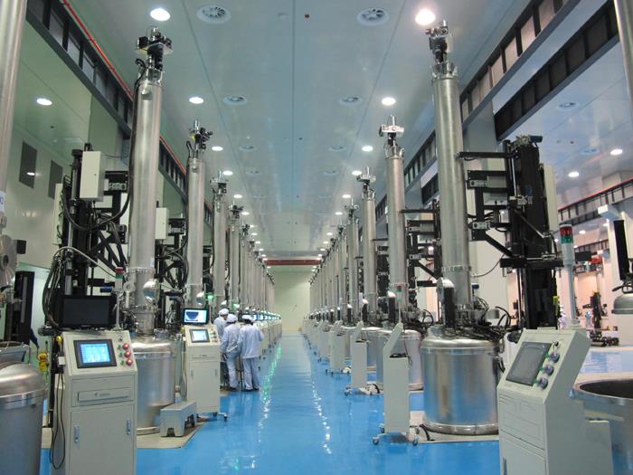
Silicon carbide (SiC) crystal growth furnaces are the cornerstone of SiC wafer production. While sharing similarities with traditional silicon crystal growth furnaces, SiC furnaces face unique challenges due to the material’s extreme growth conditions and complex defect formation mechanisms. These challenges can be broadly categorized into two areas: crystal growth and epitaxial growth.
Crystal Growth Challenges:
SiC crystal growth demands precise control over a high-temperature, enclosed environment, making monitoring and process control exceptionally difficult. Key challenges include:
(1) Thermal Field Control: Maintaining a stable and uniform temperature profile within the sealed, high-temperature chamber is crucial yet extremely challenging. Unlike the controllable melt-growth processes used for silicon, SiC crystal growth occurs above 2,000°C, making real-time monitoring and adjustment nearly impossible. Precise temperature control is paramount to achieving desired crystal properties.
(2) Polytype and Defect Control: The growth process is highly susceptible to defects like micropipes (MPs), polytype inclusions, and dislocations, each impacting crystal quality. MPs, penetrating defects several microns in size, are particularly detrimental to device performance. SiC exists in over 200 polytypes, with only the 4H structure suitable for semiconductor applications. Controlling stoichiometry, temperature gradients, growth rate, and gas flow dynamics is essential to minimize polytype inclusions. Furthermore, thermal gradients within the growth chamber can induce native stress, leading to various dislocations (basal plane dislocations (BPDs), threading screw dislocations (TSDs), threading edge dislocations (TEDs)) that impact subsequent epitaxy and device performance.
(3) Impurity Control: Achieving precise doping profiles necessitates meticulous control over external impurities. Any unintended contamination can significantly alter the electrical properties of the final crystal.
(4) Slow Growth Rate: SiC crystal growth is inherently slow compared to silicon. While a silicon ingot can be grown in 3 days, SiC requires 7 days or more, significantly impacting production efficiency and output.
Epitaxial Growth Challenges:
SiC epitaxial growth, crucial for forming device structures, demands even tighter control over process parameters:
High-Precision Control: Chamber hermeticity, pressure stability, precise gas delivery timing and composition, and strict temperature control are critical for achieving desired epitaxial layer properties. These demands become even more stringent with increasing device voltage requirements.
Uniformity and Defect Density: Maintaining uniform resistivity and low defect density in thicker epitaxial layers presents a significant challenge.
Advanced Control Systems: Sophisticated electromechanical control systems with high-precision sensors and actuators are crucial for accurate and stable parameter regulation. Advanced control algorithms capable of real-time adjustment based on process feedback are essential to navigate the complexities of SiC epitaxial growth.
Overcoming these technical hurdles is essential for unlocking the full potential of SiC technology. Continued advancements in furnace design, process control, and in-situ monitoring techniques are vital for driving the widespread adoption of this promising material in high-performance electronics.**


