
- English
- Español
- Português
- русский
- Français
- 日本語
- Deutsch
- tiếng Việt
- Italiano
- Nederlands
- ภาษาไทย
- Polski
- 한국어
- Svenska
- magyar
- Malay
- বাংলা ভাষার
- Dansk
- Suomi
- हिन्दी
- Pilipino
- Türkçe
- Gaeilge
- العربية
- Indonesia
- Norsk
- تمل
- český
- ελληνικά
- український
- Javanese
- فارسی
- தமிழ்
- తెలుగు
- नेपाली
- Burmese
- български
- ລາວ
- Latine
- Қазақша
- Euskal
- Azərbaycan
- Slovenský jazyk
- Македонски
- Lietuvos
- Eesti Keel
- Română
- Slovenski
- मराठी
- Srpski језик

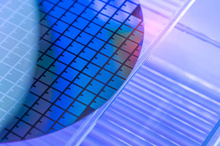
What is the Difference Between Epitaxial and Diffused Wafers
Both epitaxial and diffused wafers are essential materials in semiconductor manufacturing, but they differ significantly in their fabrication processes and target applications. This article delves into the key distinctions between these wafer types.
1. Fabrication Process:
Epitaxial wafers are manufactured by growing one or more layers of semiconductor material on a single-crystal silicon substrate. This growth process typically employs chemical vapor deposition (CVD) or molecular beam epitaxy (MBE) techniques. The epitaxial layer can be tailored with specific doping types and concentrations to achieve desired electrical properties.
Diffused wafers, on the other hand, are fabricated by introducing dopant atoms into the silicon substrate through a diffusion process. This process typically occurs at high temperatures, allowing the dopants to diffuse into the silicon lattice. The dopant concentration and depth profile in diffused wafers are controlled by adjusting the diffusion time and temperature.
2. Applications:
Epitaxial wafers are primarily used in high-performance semiconductor devices such as high-frequency transistors, optoelectronic devices, and integrated circuits. The epitaxial layer offers superior electrical characteristics like higher carrier mobility and lower defect density, crucial for these applications.
Diffused wafers are predominantly used in low-power, cost-effective semiconductor devices like low-voltage MOSFETs and CMOS integrated circuits. The simpler and less expensive fabrication process of diffusion makes it suitable for these applications.
3. Performance Differences:
Epitaxial wafers generally exhibit superior electrical properties compared to diffused wafers, including higher carrier mobility, lower defect densities, and enhanced thermal stability. These advantages make them ideal for high-performance applications.
While diffused wafers may have slightly inferior electrical properties compared to their epitaxial counterparts, their performance suffices for many applications. Additionally, their lower manufacturing cost makes them a competitive choice for low-power and cost-sensitive applications.
4. Manufacturing Cost:
The fabrication of epitaxial wafers is relatively complex, requiring sophisticated equipment and advanced technologies. Consequently, epitaxial wafers are inherently more expensive to produce.
Diffused wafers, conversely, involve a simpler fabrication process that utilizes readily available equipment and technologies, resulting in a lower manufacturing cost.
5. Environmental Impact:
The manufacturing process of epitaxial wafers can potentially generate more waste and pollutants due to the use of hazardous chemicals and high-temperature processing.
Diffused wafer fabrication, comparatively, has a lower environmental impact as it can be achieved using lower temperatures and fewer chemicals.
Conclusion:
Epitaxial and diffused wafers possess distinct characteristics in terms of fabrication process, application areas, performance, cost, and environmental impact. The choice between these two wafer types depends heavily on the specific application requirements and budget constraints.


