
- English
- Español
- Português
- русский
- Français
- 日本語
- Deutsch
- tiếng Việt
- Italiano
- Nederlands
- ภาษาไทย
- Polski
- 한국어
- Svenska
- magyar
- Malay
- বাংলা ভাষার
- Dansk
- Suomi
- हिन्दी
- Pilipino
- Türkçe
- Gaeilge
- العربية
- Indonesia
- Norsk
- تمل
- český
- ελληνικά
- український
- Javanese
- فارسی
- தமிழ்
- తెలుగు
- नेपाली
- Burmese
- български
- ລາວ
- Latine
- Қазақша
- Euskal
- Azərbaycan
- Slovenský jazyk
- Македонски
- Lietuvos
- Eesti Keel
- Română
- Slovenski
- मराठी
- Srpski језик

How to do CMP Process
2024-06-28
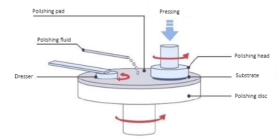
CMP process:
1. Fix the wafer at the bottom of the polishing head, and place the polishing pad on the grinding disc;
2. The rotating polishing head presses on the rotating polishing pad with a certain pressure, and a flowing grinding liquid composed of nano-abrasive particles and chemical solution is added between the silicon wafer surface and the polishing pad. The grinding liquid is evenly coated under the transmission of the polishing pad and the centrifugal force, forming a liquid film between the silicon wafer and the polishing pad;
3. Flattening is achieved through the alternating process of chemical film removal and mechanical film removal.
Main technical parameters of CMP:
Grinding rate: the thickness of the material removed per unit time.
Flatness: (the difference between the step height before and after CMP at a certain point on the silicon wafer/the step height before CMP) * 100%,
Grinding uniformity: including intra-wafer uniformity and inter-wafer uniformity. Intra-wafer uniformity refers to the consistency of grinding rates at different positions inside a single silicon wafer; inter-wafer uniformity refers to the consistency of grinding rates between different silicon wafers under the same CMP conditions.
Defect quantity: It reflects the number and type of various surface defects generated during the CMP process, which will affect the performance, reliability, and yield of semiconductor devices. Mainly including scratches, depressions, erosion, residues, and particle contamination.
CMP applications
In the entire process of semiconductor manufacturing, from silicon wafer manufacturing, wafer manufacturing, to packaging, the CMP process will need to be used repeatedly.
In the process of silicon wafer manufacturing, after the crystal rod is cut into silicon wafers, it will need to be polished and cleaned to obtain a single crystal silicon wafer like a mirror.
In the process of wafer manufacturing, through ion implantation, thin film deposition, lithography, etching, and multi-layer wiring links, in order to ensure that each layer of manufacturing surface achieves global flatness at the nanometer level, it is often necessary to use the CMP process repeatedly.
In the field of advanced packaging, CMP processes are increasingly introduced and used in large quantities, among which through silicon via (TSV) technology, fan-out, 2.5D, 3D packaging, etc. will use a large number of CMP processes.
According to the type of polished material, we divide CMP into three types:
1. Substrate, mainly silicon material
2. Metal, including aluminum/copper metal interconnect layer, Ta/Ti/TiN/TiNxCy and other diffusion barrier layers, adhesion layer.
3. Dielectrics, including interlayer dielectrics such as SiO2, BPSG, PSG, passivation layers such as SI3N4/SiOxNy, and barrier layers.
Previous:What is CMP Process


