- English
- Español
- Português
- русский
- Français
- 日本語
- Deutsch
- tiếng Việt
- Italiano
- Nederlands
- ภาษาไทย
- Polski
- 한국어
- Svenska
- magyar
- Malay
- বাংলা ভাষার
- Dansk
- Suomi
- हिन्दी
- Pilipino
- Türkçe
- Gaeilge
- العربية
- Indonesia
- Norsk
- تمل
- český
- ελληνικά
- український
- Javanese
- فارسی
- தமிழ்
- తెలుగు
- नेपाली
- Burmese
- български
- ລາວ
- Latine
- Қазақша
- Euskal
- Azərbaycan
- Slovenský jazyk
- Македонски
- Lietuvos
- Eesti Keel
- Română
- Slovenski
- मराठी
- Srpski језик

Understanding the Complete Semiconductor Device Fabrication Process
2024-06-17
1. Photolithography
Photolithography, often synonymous with pattern generation, is one of the most critical driving forces behind the rapid advancement of semiconductor technology, originating from photographic plate-making processes in printing.This technique allows the presentation of any pattern on a micro or nano-scale using photoresist, and when combined with other process technologies, transfers these patterns onto materials, realizing various designs and concepts of semiconductor materials and devices. The light source used in photolithography directly influences the precision of the patterns, with options ranging from ultraviolet, deep ultraviolet, to X-ray, and electron beams, each corresponding to increasing levels of pattern fidelity in the order mentioned.
A standard photolithography process flow includes surface preparation, adhesion, soft bake, exposure, post-exposure bake, development, hard bake, and inspection.
Surface treatment is imperative as substrates typically absorb H2O molecules from the air, which is detrimental to photolithography. Therefore, substrates initially undergo dehydration processing through baking.
For hydrophilic substrates, their adhesion to hydrophobic photoresist is insufficient, potentially causing photoresist detachment or pattern misalignment, thus the need for an adhesion promoter. Currently, hexamethyl disilazane (HMDS) and tri-methyl-silyl-diethyl-amine (TMSDEA) are widely used adhesion enhancers.
Following surface treatment, the application of photoresist begins. The thickness of the applied photoresist is not only related to its viscosity but is also affected by the spin-coating speed, generally inversely proportional to the square root of the spin speed. After coating, a soft bake is conducted to evaporate the solvent from the photoresist, improving adhesion in a process known as the prebake.
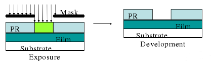
Once these steps are complete, exposure takes place. Photoresists are classified as positive or negative, with opposite properties after exposure.
Take positive photoresist as an example, where unexposed photoresist is insoluble in developer, but becomes soluble after exposure. During exposure, the light source, passing through a patterned mask, illuminates the coated substrate, patternizing the photoresist. Typically, the substrate must be aligned with the mask before exposure to control the exposure position precisely. Exposure duration must be strictly managed to prevent pattern distortion. Post-exposure, additional baking might be required to mitigate standing wave effects, although this step is optional and can be bypassed in favor of direct development. Development dissolves the exposed photoresist, transferring the mask pattern accurately onto the photoresist layer. Development time is also critical—too short leads to incomplete development, too long causes pattern distortion.
Subsequently, hard baking strengthens the attachment of the photoresist film to the substrate and improves its etch resistance. The hard bake temperature is generally slightly higher than that of the prebake.
Finally, microscopic inspection verifies if the pattern aligns with expectations. After the pattern is transferred onto the material by other processes, the photoresist has served its purpose and must be removed. Stripping methods include wet (using strong organic solvents like acetone) and dry (using oxygen plasma to etch away the film).
2. Doping Techniques
Doping is indispensable in semiconductor technology, altering the electrical properties of semiconductor materials as needed. The common doping methods include thermal diffusion and ion implantation.
(1) Ion Implantation
Ion implantation dopes the semiconductor substrate by bombarding it with high-energy ions. Compared to thermal diffusion, it has many advantages. The ions, selected by a mass analyzer, ensure high doping purity. Throughout the implantation, the substrate remains at room temperature or slightly above. Many masking films can be used, such as silicon dioxide (SiO2), silicon nitride (Si3N4), and photoresist, providing high flexibility with self-aligned mask techniques. Implant doses are precisely controlled, and the implanted impurity ion distribution is uniform within the same plane, resulting in high repeatability.
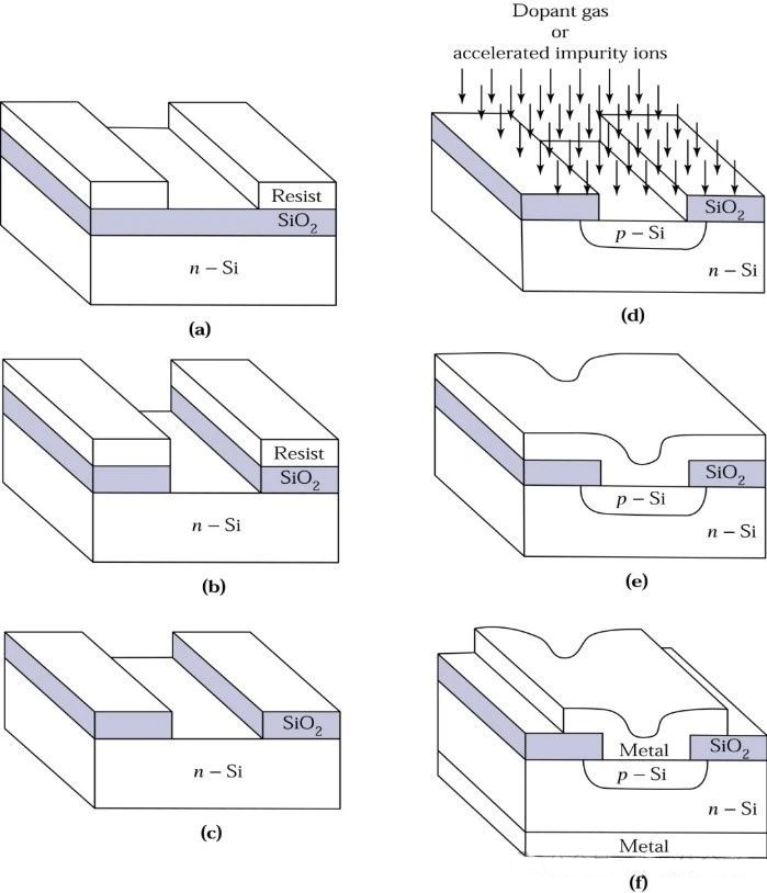
Implantation depth is determined by the energy of the ions. By regulating the energy and dose, the distribution of impurity ions in the substrate post-implantation can be manipulated. Multiple implantations with varied schemes may be performed continuously to achieve various impurity profiles. Notably, in single-crystal substrates, if the implantation direction is parallel to the crystallographic direction, channeling effects occur—some ions will travel along channels, making depth control challenging.
To prevent channeling, implantation is typically conducted at about a 7° angle to the principal axis of the single-crystal substrate or by covering the substrate with an amorphous layer.
However, ion implantation can significantly damage the crystal structure of the substrate. High-energy ions, upon collision, transfer energy to nuclei and electrons of the substrate, causing them to leave the lattice and form interstitial-vacancy defect pairs. In severe cases, the crystal structure in some regions may be destroyed, forming amorphous zones.
Lattice damage greatly affects the semiconductor material’s electrical properties, such as reducing carrier mobility or the lifetime of non-equilibrium carriers. Most importantly, the majority of implanted impurities occupy irregular interstitial sites, failing to form effective doping. Therefore, post-implantation lattice damage repair and electrical activation of impurities are essential.
(2) Rapid Thermal Processing (RTP)
Thermal annealing is the most effective method for amending lattice damage caused by ion implantation and electrically activating impurities. At high temperatures, interstitial-vacancy defect pairs in the substrate’s crystal lattice will recombine and disappear; amorphous regions will also recrystallize from the boundary with single-crystal areas via solid-phase epitaxy. To prevent the substrate material from oxidizing at high temperatures, thermal annealing must be conducted in a vacuum or inert gas atmosphere. Traditional annealing takes a long time and may cause significant impurity redistribution due to diffusion.
The advent of RTP technology addresses this issue, largely accomplishing lattice damage repair and impurity activation within a shortened annealing duration.
Depending on the heat source, RTP is categorized into several types: electron beam scanning, pulsed electron and ion beams, pulsed lasers, continuous-wave lasers, and broadband incoherent light sources (halogen lamps, graphite heaters, arc lamps), with the latter being the most widely used. These sources can heat the substrate to the required temperature in an instant, completing annealing in a short time and effectively reducing impurity diffusion.
3. Film Deposition Techniques
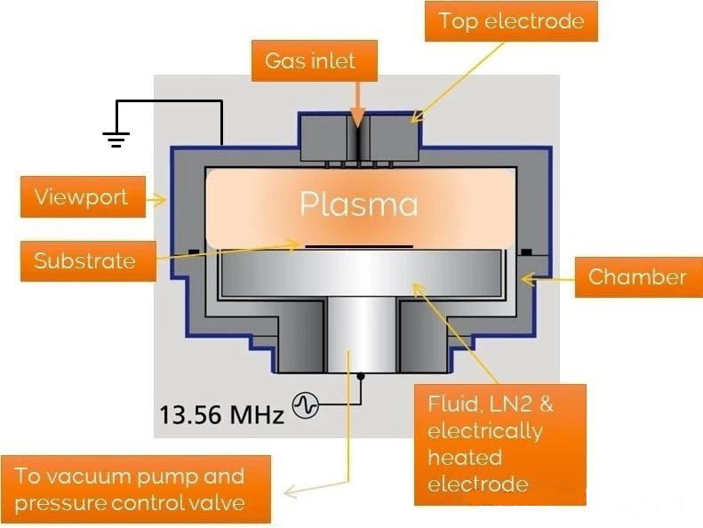
(1) Plasma-Enhanced Chemical Vapor Deposition (PECVD)
PECVD is one form of Chemical Vapor Deposition (CVD) technique for film deposition, with the other two being Atmospheric Pressure CVD (APCVD) and Low Pressure CVD (LPCVD).
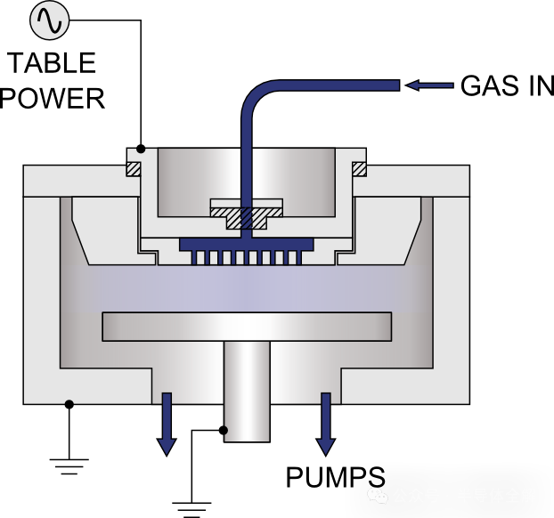
Currently, PECVD is the most widely applied among the three types. It utilizes radio frequency (RF) plasma to initiate and sustain chemical reactions at relatively low temperatures, hence facilitating low-temperature film deposition with high deposition rates. Its equipment schematic is as illustrated.
Films produced via this method exhibit exceptional adhesion and electrical properties, minimal microporosity, high uniformity, and robust small-scale fill capabilities. Factors affecting the quality of PECVD deposition include substrate temperature, gas flow rate, pressure, RF power, and frequency.
(2) Sputtering
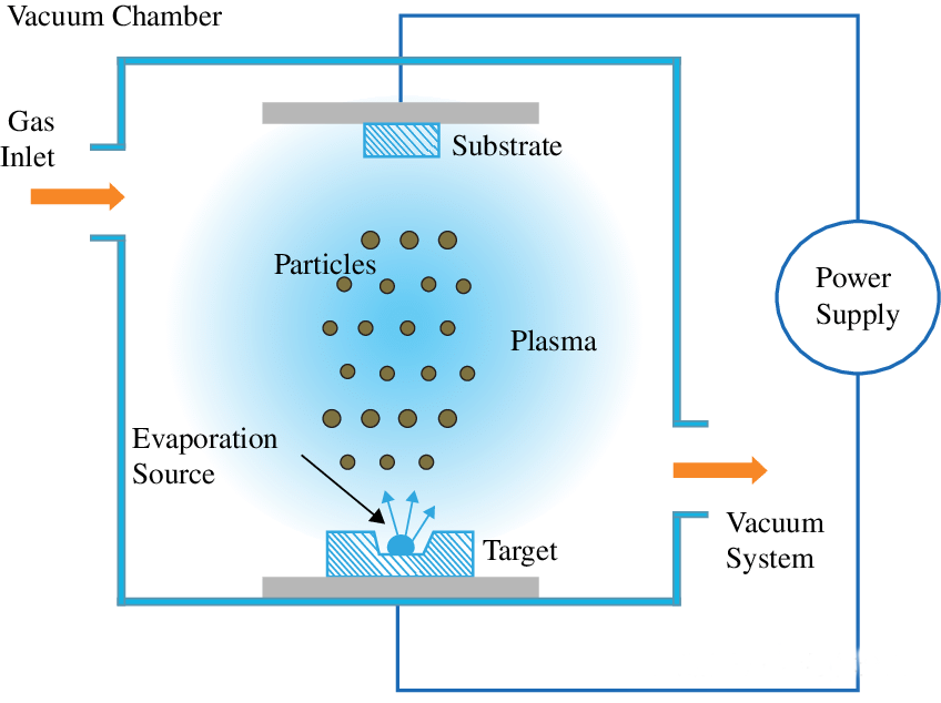
Sputtering is a Physical Vapor Deposition (PVD) method. Charged ions (commonly Argon ions, Ar+) are accelerated in an electric field, gaining kinetic energy. They are directed towards the target material, colliding with target molecules and causing them to dislodge and sputter away. These molecules also possess significant kinetic energy and move towards the substrate, depositing upon it.
Typically employed sputtering power sources include Direct Current (DC) and Radio Frequency (RF), where DC sputtering is directly applicable to conductive materials like metals, while insulating materials require RF sputtering for film deposition.
Conventional sputtering suffers from low deposition rates and high working pressures, resulting in lower film quality. Magnetron sputtering addresses these issues more ideally. It employs an external magnetic field to alter the ions’ linear trajectory to a helical path around the magnetic field direction, lengthening their path and improving collision efficiency with target molecules, thereby enhancing sputtering efficiency. This results in increased deposition rates, reduced working pressures, and significantly improved film quality.
4. Etching Techniques
Etching is classified into dry and wet modes, named for their use (or lack) of specific solutions respectively.
Typically, etching requires the preparation of a mask layer (which can directly be photoresist) to protect regions not intended for etching.
(1) Dry Etching
Common dry etching types include Inductively Coupled Plasma (ICP) etching, Ion Beam Etching (IBE), and Reactive Ion Etching (RIE).
In ICP etching, the glow discharge-produced plasma contains numerous highly chemically active free radicals (free atoms, molecules, or atomic groups), which react chemically with the target material to form volatile products, thus achieving etching.
IBE employs high-energy ions (ionized from inert gases) to directly bombard the target material’s surface for etching, representing a physical process.
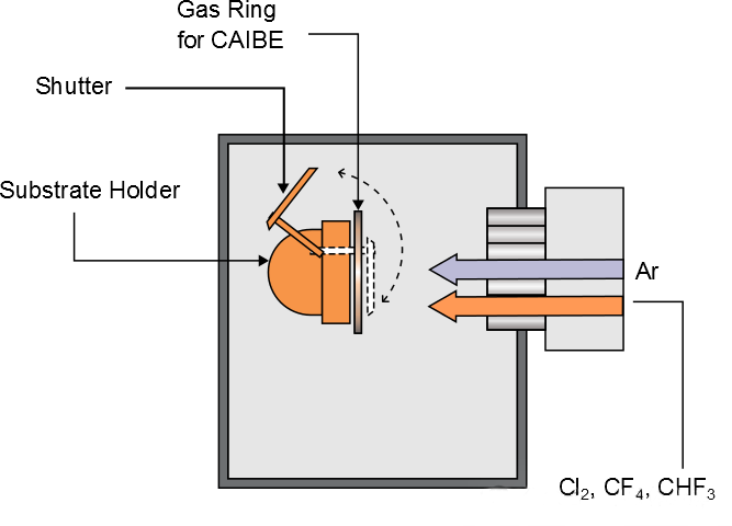
RIE is considered a combination of the previous two, replacing the inert gas used in IBE with the gas utilized in ICP etching, thereby constituting RIE.
For dry etching, the vertical etching rate far exceeds the lateral rate, i.e., it has a high aspect ratio, allowing precise replication of the mask pattern. However, dry etching also etches the mask layer, showing poorer selectivity (the ratio of etching rates of target material to the mask layer), especially with IBE, which may non-selectively etch across the material’s surface.
(2) Wet Etching
Wet etching denotes the method of etching achieved by immersing the target material in a solution (etchant) that chemically reacts with it.
This etching method is simple, cost-effective, and shows good selectivity but has a low aspect ratio. The material beneath the mask edges can be corroded, making it less precise than dry etching. To mitigate the negative impacts of a low aspect ratio, appropriate etching rates must be chosen. Factors influencing the etching rate include etchant concentration, etching time, and etchant temperature.**