- English
- Español
- Português
- русский
- Français
- 日本語
- Deutsch
- tiếng Việt
- Italiano
- Nederlands
- ภาษาไทย
- Polski
- 한국어
- Svenska
- magyar
- Malay
- বাংলা ভাষার
- Dansk
- Suomi
- हिन्दी
- Pilipino
- Türkçe
- Gaeilge
- العربية
- Indonesia
- Norsk
- تمل
- český
- ελληνικά
- український
- Javanese
- فارسی
- தமிழ்
- తెలుగు
- नेपाली
- Burmese
- български
- ລາວ
- Latine
- Қазақша
- Euskal
- Azərbaycan
- Slovenský jazyk
- Македонски
- Lietuvos
- Eesti Keel
- Română
- Slovenski
- मराठी
- Srpski језик
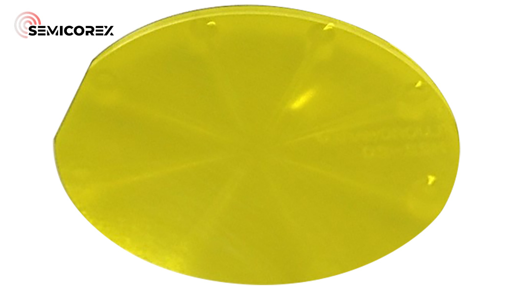
Silicon Carbide Substrate
2024-06-12
The process of silicon carbide substrate is complex and difficult to manufacture. SiC substrate occupies the main value of the industry chain, accounting for 47%. It is expected that with the expansion of production capacity and the improvement of yield in the future, it is expected to drop to 30%.
From the perspective of electrochemical properties, silicon carbide substrate materials can be divided into conductive substrates (resistivity range 15~30mΩ·cm) and semi-insulating substrates (resistivity higher than 105Ω·cm). These two types of substrates are used to manufacture discrete devices such as power devices and radio frequency devices after epitaxial growth. Among them:
1. Semi-insulating silicon carbide substrate: mainly used in the manufacture of gallium nitride radio frequency devices, optoelectronic devices, etc. By growing a gallium nitride epitaxial layer on a semi-insulating silicon carbide substrate, a silicon carbide-based gallium nitride epitaxial wafer is obtained, which can be further made into gallium nitride radio frequency devices such as HEMT.
2. Conductive silicon carbide substrate: mainly used in the manufacture of power devices. Unlike the traditional silicon power device manufacturing process, silicon carbide power devices cannot be directly manufactured on a silicon carbide substrate. It is necessary to grow a silicon carbide epitaxial layer on a conductive substrate to obtain a silicon carbide epitaxial wafer, and then manufacture Schottky diodes, MOSFETs, IGBTs and other power devices on the epitaxial layer.
The main process is divided into the following three steps:
1. Raw material synthesis: Mix high-purity silicon powder + carbon powder according to the formula, react in the reaction chamber under high temperature conditions above 2000°C, and synthesize silicon carbide particles of specific crystal form and particle size. Then through crushing, screening, cleaning and other processes, high-purity silicon carbide powder raw materials that meet the requirements are obtained.
2. Crystal growth: It is the most core process link in the manufacture of silicon carbide substrates and determines the electrical properties of silicon carbide substrates. At present, the main methods of crystal growth are physical vapor transport (PVT), high-temperature chemical vapor deposition (HT-CVD) and liquid phase epitaxy (LPE). Among them, PVT is the mainstream method for commercial growth of SiC substrates at this stage, with the highest technical maturity and the widest engineering application.
3. Crystal processing: Through ingot processing, crystal rod cutting, grinding, polishing, cleaning and other links, the silicon carbide crystal rod is processed into a substrate.


