- English
- Español
- Português
- русский
- Français
- 日本語
- Deutsch
- tiếng Việt
- Italiano
- Nederlands
- ภาษาไทย
- Polski
- 한국어
- Svenska
- magyar
- Malay
- বাংলা ভাষার
- Dansk
- Suomi
- हिन्दी
- Pilipino
- Türkçe
- Gaeilge
- العربية
- Indonesia
- Norsk
- تمل
- český
- ελληνικά
- український
- Javanese
- فارسی
- தமிழ்
- తెలుగు
- नेपाली
- Burmese
- български
- ລາວ
- Latine
- Қазақша
- Euskal
- Azərbaycan
- Slovenský jazyk
- Македонски
- Lietuvos
- Eesti Keel
- Română
- Slovenski
- मराठी
- Srpski језик
Introduction to the Silicon Carbide Ion Implantation and Annealing Process
In the doping processes of silicon carbide power devices, commonly used dopants include nitrogen and phosphorus for n-type doping, and aluminum and boron for p-type doping, with their ionization energies and solubility limits presented in Table 1 (note: hexagonal (h) and cubic (k)).

▲Table 1. Ionization Energies and Solubility Limits of Major Dopants in SiC
Figure 1 illustrates the temperature-dependent diffusion coefficients of major dopants in SiC and Si. Dopants in silicon exhibit higher diffusion coefficients, allowing for high-temperature diffusion doping around 1300°C. In contrast, the diffusion coefficients of phosphorus, aluminum, boron, and nitrogen in silicon carbide are significantly lower, necessitating temperatures above 2000°C for reasonable diffusion rates. High-temperature diffusion introduces various issues, such as multiple diffusion defects degrading electrical performance and the incompatibility of common photoresists as masks, making ion implantation the sole choice for silicon carbide doping.

▲Figure 1. Comparative Diffusion Constants of Major Dopants in SiC and Si
During ion implantation, ions lose energy through collisions with lattice atoms of the substrate, transferring energy to these atoms. This transferred energy releases the atoms from their lattice binding energy, allowing them to move within the substrate and collide with other lattice atoms, dislodging them. This process continues until no free atoms have sufficient energy to release others from the lattice.
Due to the massive quantity of ions involved, ion implantation causes extensive lattice damage near the substrate surface, with the extent of damage related to the implantation parameters such as dosage and energy. Excessive dosages can destroy the crystal structure near the substrate surface, turning it amorphous. This lattice damage must be repaired to a single-crystal structure and activate the dopants during the annealing process.
High-temperature annealing allows atoms to gain energy from heat, undergoing rapid thermal motion. Once they move to positions within the single-crystal lattice with the lowest free energy, they settle there. Thus, the damaged amorphous silicon carbide and dopant atoms near the substrate interface reconstruct the single-crystal structure by fitting into the lattice positions and being bound by lattice energy. This simultaneous lattice repair and dopant activation occur during annealing.
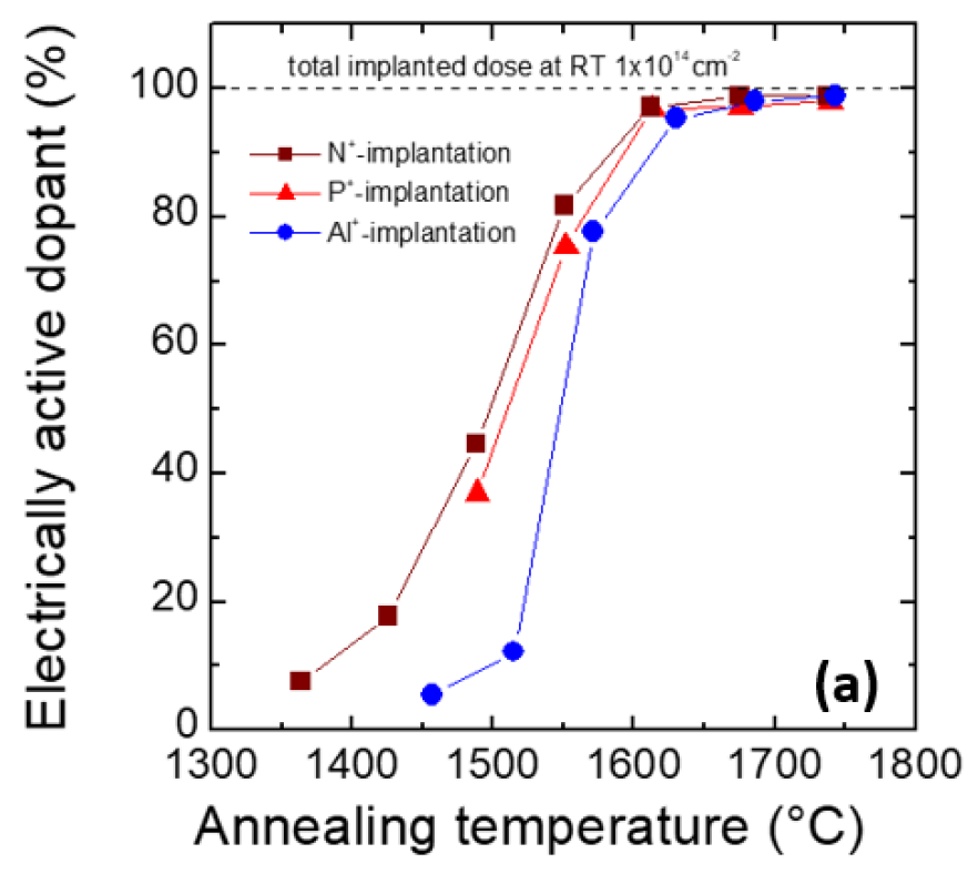
Research has reported the relationship between the activation rates of dopants in SiC and annealing temperatures (Figure 2a). In this context, both the epitaxial layer and substrate are n-type, with nitrogen and phosphorus implanted to a depth of 0.4μm and a total dosage of 1×10^14 cm^-2. As shown in Figure 2a, nitrogen exhibits an activation rate below 10% after annealing at 1400°C, reaching 90% at 1600°C. The behavior of phosphorus is similar, requiring an annealing temperature of 1600°C for a 90% activation rate.

▲Figure 2a. Activation Rates of Different Elements at Various Annealing Temperatures in SiC
For p-type ion implantation processes, aluminum is generally used as the dopant due to boron’s anomalous diffusion effect. Similar to n-type implantation, annealing at 1600°C significantly enhances aluminum’s activation rate. However, research by Negoro et al. found that even at 500°C, the sheet resistance reached saturation at 3000Ω/square with high-dose aluminum implantation, and increasing the dosage further did not reduce the resistance, indicating that aluminum no longer ionizes. Thus, using ion implantation to create heavily doped p-type regions remains a technological challenge.

▲Figure 2b. Relationship Between Activation Rates and Dosage of Different Elements in SiC
The depth and concentration of dopants are critical factors in ion implantation, directly affecting the subsequent electrical performance of the device and must be strictly controlled. Secondary Ion Mass Spectrometry (SIMS) can be utilized to measure the depth and concentration of dopants post-implantation.**


