- English
- Español
- Português
- русский
- Français
- 日本語
- Deutsch
- tiếng Việt
- Italiano
- Nederlands
- ภาษาไทย
- Polski
- 한국어
- Svenska
- magyar
- Malay
- বাংলা ভাষার
- Dansk
- Suomi
- हिन्दी
- Pilipino
- Türkçe
- Gaeilge
- العربية
- Indonesia
- Norsk
- تمل
- český
- ελληνικά
- український
- Javanese
- فارسی
- தமிழ்
- తెలుగు
- नेपाली
- Burmese
- български
- ລາວ
- Latine
- Қазақша
- Euskal
- Azərbaycan
- Slovenský jazyk
- Македонски
- Lietuvos
- Eesti Keel
- Română
- Slovenski
- मराठी
- Srpski језик
Substrate Cutting and Grinding Process
2024-04-01
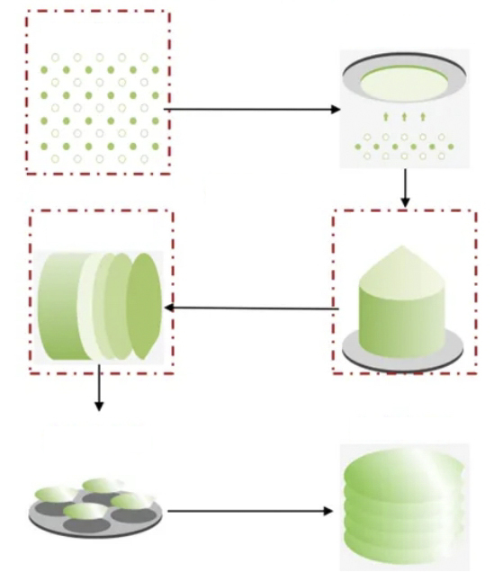
SiC substrate material is the core of SiC chip. The production process of the substrate is: after obtaining the SiC crystal ingot through single crystal growth; then preparing the SiC substrate requires smoothing, rounding, cutting, grinding (thinning); mechanical polishing, chemical mechanical polishing; and cleaning, testing, etc. Process
There are three main methods of crystal growth: physical vapor transport (PVT), high temperature chemical vapor deposition (HT-CVD) and liquid phase epitaxy (LPE). The PVT method is the mainstream method for commercial growth of SiC substrates at this stage. The growth temperature of SiC crystal is above 2000°C, which requires high temperature and pressure control. Currently, there are problems such as high dislocation density and high crystal defects.
Substrate cutting cuts the crystal ingot into wafers for subsequent processing. The cutting method affects the coordination of subsequent grinding and other processes of silicon carbide substrate wafers. Ingot cutting is mainly based on mortar multi-wire cutting and diamond wire saw cutting. Most existing SiC wafers are cut by diamond wire. However, SiC has high hardness and brittleness, which results in low wafer yield and high consumable cost of cutting wires. Advanced questions. At the same time, the cutting time of 8-inch wafers is significantly longer than that of 6-inch wafers, and the risk of cutting lines getting stuck is also higher, resulting in a decrease in yield.

The development trend of substrate cutting technology is laser cutting, which forms a modified layer inside the crystal and peels off the wafer from the silicon carbide crystal. It is a non-contact processing without material loss and no mechanical stress damage, so the loss is lower, the yield is higher, and the processing The method is flexible and the surface shape of SiC processed is better.
SiC substrate grinding processing includes grinding (thinning) and polishing. The planarization process of SiC substrate mainly includes two process routes: grinding and thinning.
Grinding is divided into rough grinding and fine grinding. The mainstream rough grinding process solution is a cast iron disc combined with single crystal diamond grinding fluid. After the development of polycrystalline diamond powder and polycrystalline-like diamond powder, the silicon carbide fine grinding process solution is a polyurethane pad combined with a polycrystalline-like fine grinding fluid. The new process solution is honeycomb polishing pad combined with agglomerated abrasives.
Thinning is divided into two steps: rough grinding and fine grinding. The solution of thinning machine and grinding wheel is adopted. It has a high degree of automation and is expected to replace the grinding technical route. The thinning process solution is streamlined, and the thinning of high-precision grinding wheels can save single-sided mechanical polishing (DMP) for the polishing ring; the use of grinding wheels has fast processing speed, strong control over the processing surface shape, and is suitable for large-size wafer processing. At the same time, compared to the double-sided processing of grinding, thinning is a single-sided processing process, which is a key process for grinding the back side of the wafer during epitaxial manufacturing and wafer packaging. The difficulty in promoting the thinning process lies in the difficulty of research and development of grinding wheels and the high manufacturing technology requirements. The degree of localization of grinding wheels is very low, and the cost of consumables is high. Currently, the grinding wheel market is mainly occupied by DISCO.
Polishing is used to smooth the SiC substrate, eliminate surface scratches, reduce roughness and eliminate processing stress. It is divided into two steps: rough polishing and fine polishing. Alumina polishing liquid is often used for rough polishing of silicon carbide, and aluminum oxide polishing liquid is mostly used for fine polishing. Silicon oxide polishing fluid.


