- English
- Español
- Português
- русский
- Français
- 日本語
- Deutsch
- tiếng Việt
- Italiano
- Nederlands
- ภาษาไทย
- Polski
- 한국어
- Svenska
- magyar
- Malay
- বাংলা ভাষার
- Dansk
- Suomi
- हिन्दी
- Pilipino
- Türkçe
- Gaeilge
- العربية
- Indonesia
- Norsk
- تمل
- český
- ελληνικά
- український
- Javanese
- فارسی
- தமிழ்
- తెలుగు
- नेपाली
- Burmese
- български
- ລາວ
- Latine
- Қазақша
- Euskal
- Azərbaycan
- Slovenský jazyk
- Македонски
- Lietuvos
- Eesti Keel
- Română
- Slovenski
- मराठी
- Srpski језик
About defects in SiC crystals - Micropipe
2023-08-18
SiC substrate can have microscopic defects, such as Threading Screw Dislocation (TSD), Threading Edge Dislocation (TED), Base Plane Dislocation (BPD), and others. These defects are caused by deviations in the arrangement of atoms at the atomic level. SiC crystals may also have macroscopic dislocations, like Si or C inclusions, micropipe, hexagonal voids, polymorphs, etc. These dislocations are typically large in size.

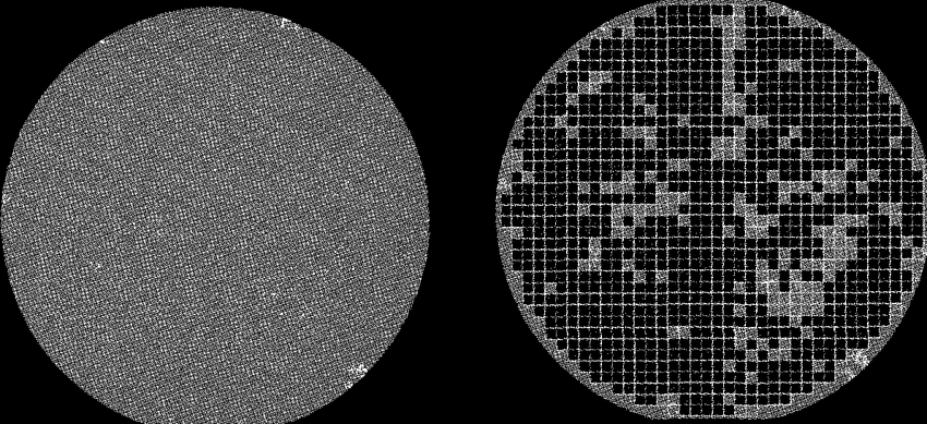
One of the major issues in manufacturing SiC devices is three-dimensional microstructures known as "micropipe" or "pinholes", which are typically 30-40um and 0.1-5um in size respectively. These micropipe have a density of 10-10³/cm² and can penetrate the epitaxial layer, resulting in device-killer defects. They are primarily caused by the clustering of spiro dislocations and are considered the primary obstacle in the development of SiC devices.
Microtubule defects on the substrate are the source of other defects formed in the epitaxial layer during the growth process, such as voids, inclusions of various polymorphs, twins, etc. Therefore, the most important thing to do during the growth process of the substrate material for high-voltage and high-power SiC devices is to reduce the formation of microtubule defects in bulk SiC crystals and to prevent them from entering the epitaxial layer.
The micropipe can be viewed as small pits, and by optimizing the conditions of the process we can "fill in the pits" to reduce the density of the micropipe. Several studies in the literature and experimental data have shown that evaporation epitaxy, CVD growth, and liquid-phase epitaxy can fill in the micropipe and reduce the formation of micropipe and dislocations.
Semicorex utilizes the MOCVD technique to create SiC coatings that effectively decrease micropipe density, resulting in top-quality products. If you have any inquiries or need additional details, please don't hesitate to get in touch with us.
Contact phone # +86-13567891907
Email: sales@semicorex.com


